Y-Sb-Te phase-change material, phase-change memory unit and preparation method thereof

A phase-change memory and phase-change material technology, applied in the field of semiconductor material preparation, can solve the problems of poor data retention, low crystallization temperature, and low high-to-low resistance ratio, and achieve fast crystallization speed, adjustable composition, and high deposition. The effect of state stability

Inactive Publication Date: 2018-03-06
SHANGHAI INST OF MICROSYSTEM & INFORMATION TECH CHINESE ACAD OF SCI
View PDF9 Cites 7 Cited by
  • Summary
  • Abstract
  • Description
  • Claims
  • Application Information

AI Technical Summary

Problems solved by technology

[0005] In view of the above-mentioned shortcoming of the prior art, the object of the present invention is to provide a kind of Y-Sb-Te phase-change material, phase-change memory unit and preparation method thereof, for solving the problem of Sb in the prior art x Te y Phase change materials have problems such as low crystallization temperature, poor data retention ability, and small high-to-low resistance ratio.

Method used


Image

  • Y-Sb-Te phase-change material, phase-change memory unit and preparation method thereof
  • Y-Sb-Te phase-change material, phase-change memory unit and preparation method thereof

Examples


Embodiment 1

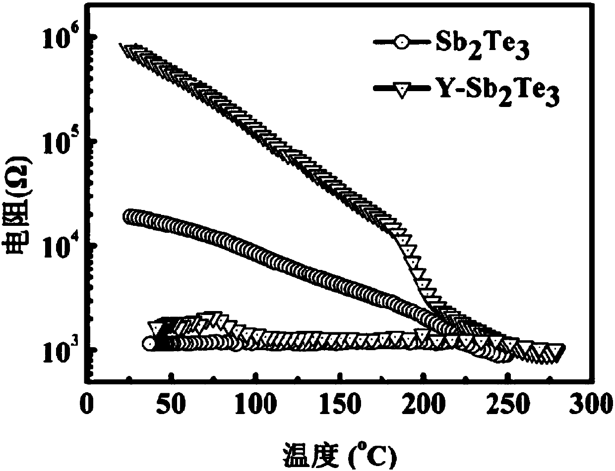
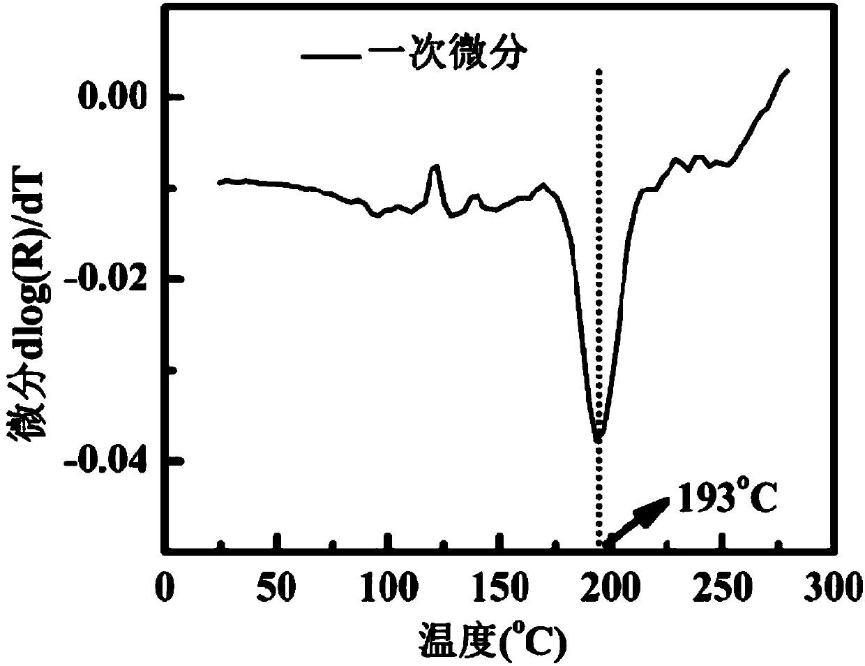
[0033] In this example, Y 100-x-y Sb x Te y (x / y=2 / 3) phase change material, and test it to further illustrate a technical solution of the present invention. The specific preparation plan is as follows:

[0034] Prepare Y on the silicon substrate and the thermally oxidized silicon substrate by using the dual-target co-sputtering method in magnetron sputtering 100-x-y Sb x Te y Phase change material, where 0 <100-x-y <50, 0.5≤x / y≤4. The prepared Y-Sb-Te series phase change material is a thin film material, and the thickness of the thin film can be controlled at 100nm~250nm by adjusting the long film time.

[0035] Specifically, it includes the following steps: under an argon atmosphere, using Sb 2 Te 3 Alloy target and Y elemental target are co-sputtered. Among them, Sb 2 Te 3 The alloy target uses a DC power supply, and the Y single-mass target uses a radio frequency power supply; by changing the radio frequency power to adjust the atomic percentage of Y, a Y-Sb-Te series of phase ...

Embodiment 2

[0040] In this example, Y 100-x-y Sb x Te y (x / y=2 / 1) phase change material, and test it to further illustrate a technical solution of the present invention. The specific preparation plan is as follows:

[0041] Prepare Y on the silicon substrate and the thermally oxidized silicon substrate by using the three-target co-sputtering method in magnetron sputtering 100-x-y Sb x Te y Phase change material, where 0 <100-x-y <50, 0.5≤x / y≤4. The prepared Y-Sb-Te series phase change material is a thin film material, and the thickness of the thin film can be controlled at 100nm~250nm by adjusting the long film time.

[0042] Specifically, it includes the following steps: under an argon atmosphere, using Sb 2 Te 3 Alloy target, Sb elemental target and Y elemental target are co-sputtered with three targets. Among them, Sb 2 Te 3 The alloy target and the Sb elementary target use a DC power supply, and the Y elementary target uses a radio frequency power supply; by changing the radio frequency po...

Embodiment 3

[0047] In this example, Y 100-x-y Sb x Te y (x / y=1 / 2) phase change material, and test it to further illustrate a technical solution of the present invention. The specific preparation plan is as follows:

[0048] Prepare Y on the silicon substrate and the thermally oxidized silicon substrate by using the three-target co-sputtering method in magnetron sputtering 100-x-y Sb x Te y Phase change material, where 0 <100-x-y <50, 0.5≤x / y≤4. The prepared Y-Sb-Te series phase change material is a thin film material, and the thickness of the thin film can be controlled at 100nm~250nm by adjusting the long film time.

[0049] Specifically, it includes the following steps: under an argon atmosphere, using Sb 2 Te 3 Alloy target, Te elemental target and Y elemental target are co-sputtered with three targets. Among them, Sb 2 Te 3 The alloy target and the Te elementary target use a DC power supply, and the Y elementary target uses a radio frequency power supply; by changing the radio frequency po...


PUM

PropertyMeasurementUnit
thicknessaaaaaaaaaa

Abstract

The invention provides a Y-Sb-Te phase-change material, a phase-change memory unit and a preparation method thereof. The Y-Sb-Te phase-change material is a compound comprising three elements includingyttrium, antimony and tellurium. The chemical formula of the Y-Sb-Te phase-change material is Y100-x-ySbxTey, wherein 0<100-x-y<50, and 0.1<=x/y<=4. According to the invention, the Y-Sb-Te-series phase-change material is faster in crystallization speed and higher in deposition-state stability. Under the action of electric pulses, the reversible phase-change of the material can be realized. Beforeand after the phase-change process, the material is different in resistance and the resistance difference of the material is large, wherein 0 and 1 can be distinguished. Therefore, the material is anideal phase-change material and can be used for preparing the phase-change memory unit. The Y-Sb-Te-series phase-change material can be prepared by a plurality of methods, wherein the magnetron sputtering method is flexible to apply and can conveniently prepare a Y100-x-ySbxTey composite thin film adjustable in component and high in quality.

Description

Technical field [0001] The invention relates to the technical field of semiconductor material preparation, in particular to a Y-Sb-Te phase change material, a phase change memory cell and a preparation method thereof. Background technique [0002] Memory is an important part of the current semiconductor market and the cornerstone of information technology. It plays an important role in life and in the national economy. At present, the storage products of memory mainly include: flash memory, magnetic disk, dynamic memory, static memory and other non-volatile technologies: ferroelectric RAM, magnetic RAM, carbon nanotube RAM, resistive RAM, copper RAM (CopperBridge), holographic Storage, single-electron storage, molecular storage, polymer storage, racetrack memory, probe memory, etc. as candidates for next-generation memory have also been extensively studied. Each of these technologies has its own characteristics, but most of them are still in the stage of theoretical research or ...

Claims


Application Information

Patent Timeline
Patent Type & Authority Applications(China)
IPC IPC(8): H01L45/00
CPCH10N70/881H10N70/026
Inventor 王勇饶峰宋志棠吴良才丁科元李涛
Owner SHANGHAI INST OF MICROSYSTEM & INFORMATION TECH CHINESE ACAD OF SCI
Why Eureka
Try Eureka