Alloy thermoelectric semiconductor material and fabrication method thereof

A technology of thermoelectric semiconductors and bulk materials, applied in the direction of thermoelectric device junction lead-out materials, thermoelectric device manufacturing/processing, etc., can solve the problems of reduced lattice thermal conductivity and difficulty in achieving a large-scale leap in carrier concentration, etc. , to achieve the effects of reduced formation, reduced carrier concentration, and optimized carrier concentration

Active Publication Date: 2018-03-13
TONGJI UNIV
View PDF4 Cites 11 Cited by
  • Summary
  • Abstract
  • Description
  • Claims
  • Application Information

AI Technical Summary

Problems solved by technology

However, this method is often limited by the limited solubility of doping elements in the matrix. The low doping level not only makes it difficult to achieve a wide range of carrier concentration, but also introduces a small amount of point defects that cannot make the lattice thermal conductivity of the matrix material. reduced to a very low level

Method used


Image

  • Alloy thermoelectric semiconductor material and fabrication method thereof
  • Alloy thermoelectric semiconductor material and fabrication method thereof
  • Alloy thermoelectric semiconductor material and fabrication method thereof

Examples


Embodiment 1

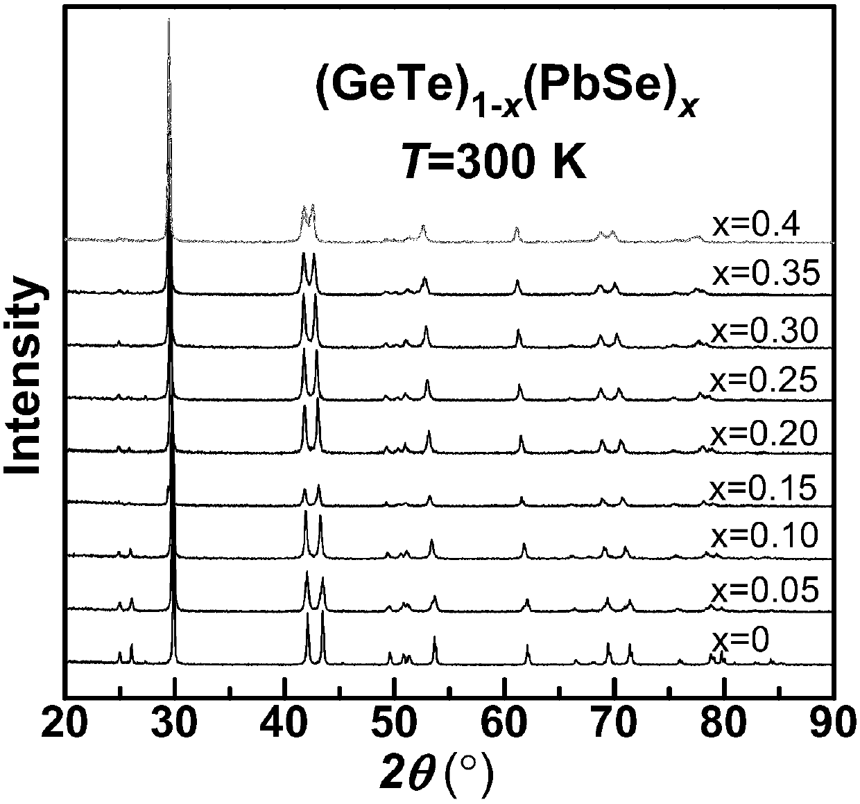
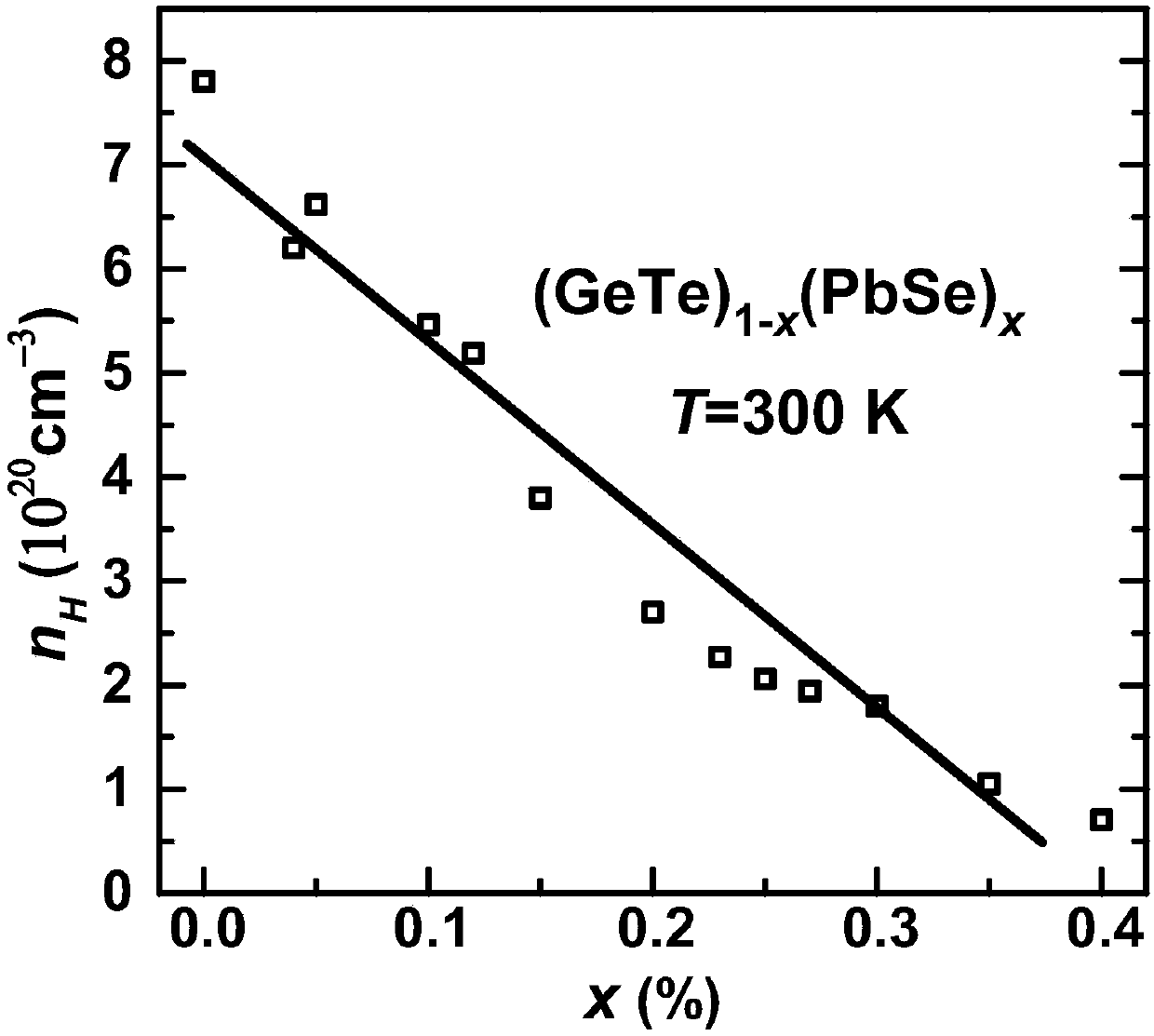
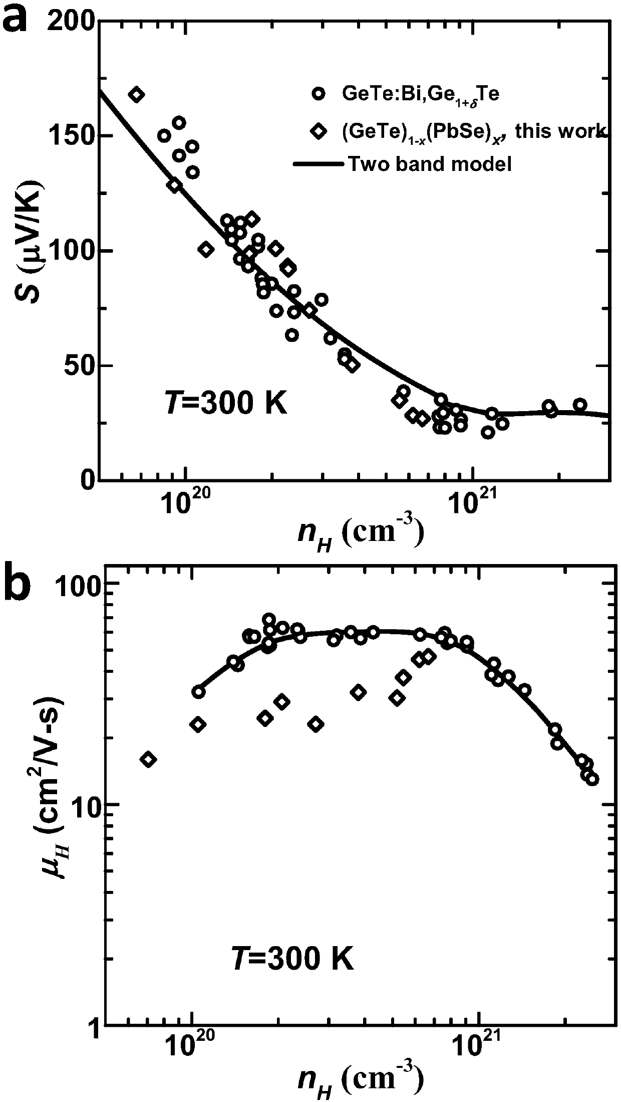
[0043] A kind of GeTe matrix alloy semiconductor thermoelectric material, its chemical formula is (GeTe) 1-x (PbSe) x, 01-x (PbSe) x Block material:

[0044] (1) According to different x values, the chemical formula is (GeTe) 1-x (PbSe) x The stoichiometric ratio of (x=0~0.4) Weigh the elemental raw materials germanium Ge, tellurium Te, lead Pb, selenium Se with a purity greater than 99.99%, place the raw materials in a quartz ampoule, and seal the quartz ampoule under vacuum.

[0045] (2) Hang the quartz tube containing the raw materials in a high-temperature well-type furnace, slowly raise the temperature to 900-1000°C at a rate of 150-200°C per hour, and keep it warm for 6-12 hours, and then quickly quench and cool to obtain the first ingot ; In this step of this embodiment, the temperature is slowly raised to 950° C. at a rate of 200° C. per hour, and kept at 950° C. for 6 hours.

[0046] (3) heat-treat the first ingot after high-temperature melting and quenching obta...

Embodiment 2

[0051] The preparation method of this embodiment is specifically:

[0052] A method for preparing a high-performance GeTe-based alloy thermoelectric semiconductor material, comprising the following steps:

[0053] (1) Vacuum packaging: The elemental elements Ge, Te, Pb and Se with a purity greater than 99.99% are dosed according to the stoichiometric ratio, and loaded into quartz ampoules in order of density from small to large, and then packaged after vacuuming for 30 minutes with a mechanical pump ;

[0054] (2) Melting and quenching: Put the quartz ampoule containing the raw material into the pit furnace and heat slowly, and raise the temperature of the quartz ampoule from room temperature to 900°C at a rate of 150°C per hour and keep it warm for 12 hours to make the raw material react in a molten state. This is followed by quenching in cold water to obtain the first ingot.

[0055] (3) Annealing and quenching: put the first ingot in the quartz ampoule into the well furna...

Embodiment 3

[0059] The preparation method of this embodiment is specifically:

[0060] A method for preparing a high-performance GeTe-based alloy thermoelectric semiconductor material, comprising the following steps:

[0061] (1) Vacuum packaging: The elemental elements Ge, Te, Pb and Se with a purity greater than 99.99% are dosed according to the stoichiometric ratio, and loaded into quartz ampoules in order of density from small to large, and then packaged after vacuuming for 30 minutes with a mechanical pump ;

[0062] (2) Melting quenching: Put the quartz ampoule containing the raw material into the pit furnace and heat it slowly, raise the temperature of the quartz ampoule from room temperature to 1000°C at a rate of 200°C per hour and keep it warm for 6 hours to make the raw material react in a molten state, This is followed by quenching in cold water to obtain the first ingot.

[0063] (3) Annealing and quenching: put the first ingot in the quartz ampoule into the pit furnace and...


PUM

PropertyMeasurementUnit
thermoelectric figure of meritaaaaaaaaaa

Abstract

The invention relates to an alloy thermoelectric semiconductor material and a fabrication method thereof. The chemical formula of the alloy thermoelectric semiconductor material is (GeTe)<1-x>(PbSe)<x>, and x is more than 0 but less than0.4. During fabrication, simple elements Ge, Te, Pb and Se are sequentially loaded in a quartz ampoule from small to large and are packaged after vacuumizing, andthe steps of melting quenching, annealing quenching and hot-press sintering are sequentially performed to finally fabricate the alloy thermoelectric semiconductor material. Compared with the prior art, substitution of the elements (Ge/Pb and Te/Se) in the main group are performed on positions of a negative ion and a positive ion in a GeTe material, the large-range control of carrier concentrationis achieved, the carrier concentration level of the GeTe material is optimized, meanwhile, the thermoelectric merit figure of the material is also increased by point defect introduced by element substitution, the lattice thermal conduction of the material is substantially reduced as well as the carrier concentration is regulated, and a new idea is provided for improvement of thermoelectric performance of a GeTe-based thermoelectric material and same-type material.

Description

technical field [0001] The invention relates to the technical field of new energy materials, in particular to an alloy thermoelectric semiconductor material and a preparation method thereof. Background technique [0002] With the continuous reduction of traditional fossil fuels on the earth, environmental pollution and energy crisis have become increasingly prominent, the demand for clean and renewable energy is very urgent. Thermoelectric materials can realize mutual conversion of heat and electricity, based on the Seebeck effect or Peltier effect, and can be used as generators or refrigerators, respectively. The working medium in thermoelectric materials is the inherent carrier of the material, so it can be used as a noiseless, zero-emission, and environmentally friendly energy direct conversion tool, and plays an important role in the utilization of industrial waste heat and automobile exhaust waste heat. [0003] The energy conversion efficiency of thermoelectric materi...

Claims


Application Information

Patent Timeline
Patent Type & Authority Applications(China)
IPC IPC(8): H01L35/16H01L35/34
CPCH10N10/852H10N10/01
Inventor 裴艳中李文李娟
Owner TONGJI UNIV
Why Eureka
Try Eureka