Three-crystal overcurrent protection type A circuit voltage regulating chip in unloading low-overvoltage zone
A technology of overvoltage area and load dumping, applied in the direction of adjusting electrical variables, control/regulation systems, instruments, etc., can solve the problems of high cost of electronic modules, impact on driving safety, failure or breakdown, and achieve simple structure and low cost , high pressure effect
- Summary
- Abstract
- Description
- Claims
- Application Information
AI Technical Summary
Problems solved by technology
Method used
Image
Examples
Embodiment 1
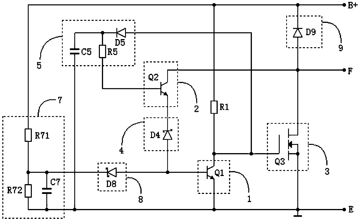
[0032] Such as figure 1 As shown, it is the first three-crystal overcurrent protection type A circuit voltage regulator chip in the load dump low overvoltage region. Its structural features include:
[0033] First transistor 1 (Q1), second transistor 2 (Q2), third transistor 3 (Q3), energy storage delay unit 5, threshold adjustment unit 4, resistor R1, sampling unit 7, reference unit 8 and freewheeling unit 9, of which:
[0034] The emitter of the first transistor Q1 is grounded, the collector of the first transistor is connected to the positive pole B+ of the power supply through the resistor R1, and the collector of the first transistor is also connected to the input terminal (gate) of the third transistor Q3 and the input of the energy storage delay unit 5 terminal, the ground terminal (source) of the third transistor Q3 is grounded (that is, E, the same below), the output terminal (drain) of the third transistor Q3 is connected to the collector of the second transistor Q2...
Embodiment 2
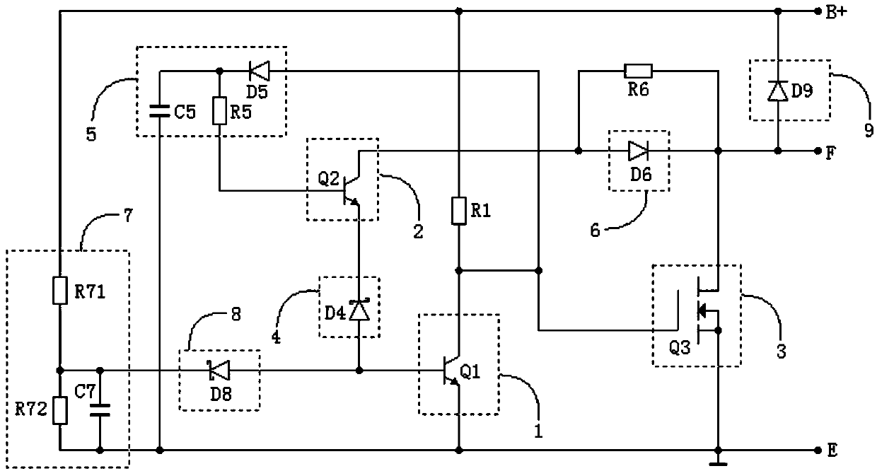
[0045] On the basis of the above-mentioned embodiment 1, the embodiment of the present invention also provides a three-crystal overcurrent protection type A circuit voltage regulation chip in the load dump low overvoltage region, such as figure 2 As shown, the circuit in the above figure 1 The collector loop of the second transistor Q2 in the circuit shown is connected to the diode 6 (D6) and the resistor R6, the anode of the diode D6 is connected to the collector of the second transistor Q2 and one end of the resistor R6 at the same time, and the cathode of the diode D6 is connected to the output of the third transistor Q3 terminal (drain), and the other terminal of the resistor R6 is connected to the output terminal of the third transistor Q3. Its working process is the same as the above figure 1 The circuit shown is basically the same, only when the power tube Q3 is normally turned on, the collector potential of the triode Q2 is pulled down through the diode D6. At this t...
Embodiment 3
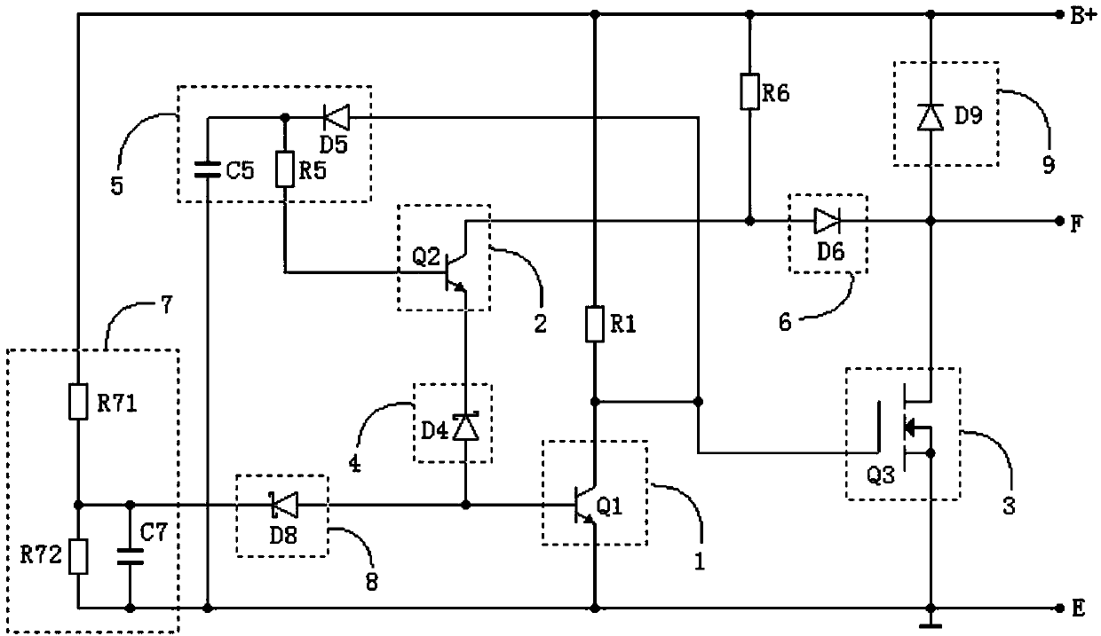
[0047] Also on the basis of the above-mentioned embodiment 1, the embodiment of the present invention also provides a three-crystal overcurrent protection type A circuit voltage regulation chip in the load dump low overvoltage region, such as image 3 As shown, the circuit in the above figure 1 In the circuit shown, the collector circuit of the second transistor Q2 is connected in series with a diode D6, and a resistor R6 is also added. The anode of the diode D6 is connected to the collector of the second transistor Q2 and one end of the resistor R6 at the same time, and the cathode of the diode D6 is connected to the third transistor Q3 The output terminal (drain), the other end of the resistor R6 is connected to the positive pole of the power supply. Its working process is also the same as the above figure 1 The circuit shown is basically the same, only when the power tube Q3 is normally turned on, the collector potential of the triode Q2 is pulled down through the diode D6...
PUM
 Abstract
Description
Claims
Application Information


