

High-density embedded line making method
A production method and embedded technology, applied in printed circuit manufacturing, printed circuit, photolithography/patterning, etc., can solve problems such as fineness and stability, deformation, etc.
- Summary
- Abstract
- Description
- Claims
- Application Information
AI Technical Summary
Problems solved by technology
Method used
Image

Examples
Embodiment 1
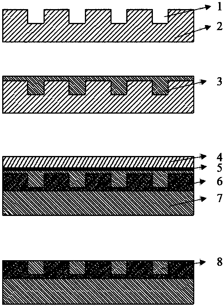
[0041] (1) Structural motherboard
[0042] (1a) Clean the surface of the stainless steel plate with deionized water in an ultrasonic cleaner for 5 minutes, and then put it into a vacuum drying oven for drying treatment.
[0043] (1b) Input the pre-designed circuit pattern into the laser equipment, and cut the circuit pattern on the surface of the stainless steel plate by laser cutting. The line width and line spacing of the circuit pattern are both 2 μm, and the depth is 5 μm.
[0044] (1c) Perform surface plasma cleaning on the cut stainless steel plate for 8 minutes.
[0045] (2) Copper plating
[0046] The stainless steel plate with the circuit pattern cut out is connected to the negative circuit, and copper plating is performed on the groove of the circuit pattern. The copper layer generated during the copper plating process fills the groove of the circuit pattern, thereby obtaining the copper layer of the circuit. In this embodiment, the deposition rate of the copper la...
Embodiment 2
[0054] (1) Structural motherboard
[0055] (1a) Clean the surface of the stainless steel plate with deionized water in an ultrasonic cleaner for 5 minutes, and then put it into a vacuum drying oven for drying treatment.
[0056] (1b) Input the pre-designed circuit pattern into the electron beam equipment, and cut the circuit pattern on the surface of the stainless steel plate by electron beam cutting. The line width of the circuit pattern is 1 μm, the line spacing is 2 μm, and the depth is 6 μm.
[0057] (1c) Perform surface plasma cleaning on the cut stainless steel plate for 10 min.
[0058] (2) Copper plating
[0059] The stainless steel plate with the circuit pattern cut out is connected to the negative circuit, and copper plating is performed on the groove of the circuit pattern. The copper layer generated during the copper plating process fills the groove of the circuit pattern, thereby obtaining the copper layer of the circuit. In this embodiment, the deposition rate ...
PUM
| Property | Measurement | Unit |
|---|---|---|
| Line width | aaaaa | aaaaa |
| Thickness | aaaaa | aaaaa |
| Thickness | aaaaa | aaaaa |
Abstract
Description
Claims
Application Information