tsv plating method

A technology of electroplating solution and current value, applied in circuits, semiconductor devices, etc., can solve problems such as the influence of rewiring process semiconductor device production

Active Publication Date: 2019-08-23
WUHAN XINXIN SEMICON MFG CO LTD
View PDF5 Cites 0 Cited by
  • Summary
  • Abstract
  • Description
  • Claims
  • Application Information

AI Technical Summary

Problems solved by technology

like figure 1 Among them, the TSV structure (including the filled through-silicon hole and the trench connected with it) has a pit 10 formed on the surface directly above the through-silicon hole, and its existence will affect the subsequent rewiring process and semiconductor device manufacturing.

Method used


Image

  • tsv plating method
  • tsv plating method
  • tsv plating method

Examples


Embodiment Construction

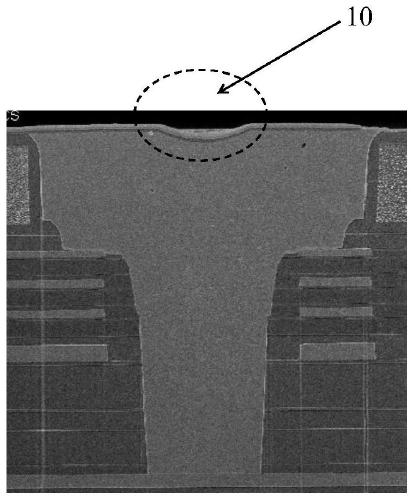
[0030] At present, in the TSV process of integrated circuits, it is usually necessary to fill small-sized TSVs (bottom pore diameters of about 20-100 nm), large-sized TSVs (bottom pore diameters greater than 1 μm) and trenches above TSVs. The filler metal is copper (Cu). However, the applicant found that using the current TSV electroplating method, especially for large-sized TSVs, pits are formed on the surface of the TSV structure after electroplating. After measurement, the depth of the pits is even It will reach 6-10μm, so it cannot be removed even if the subsequent CMP process is performed, such as figure 1 The pit 10 in is the pit that still remains after the CMP process. The existence of the pits 10 will affect the flatness of the silicon substrate, and will affect the subsequent redistribution layer (Redistribution Layer, RDL) layer and the fabrication of semiconductor devices.

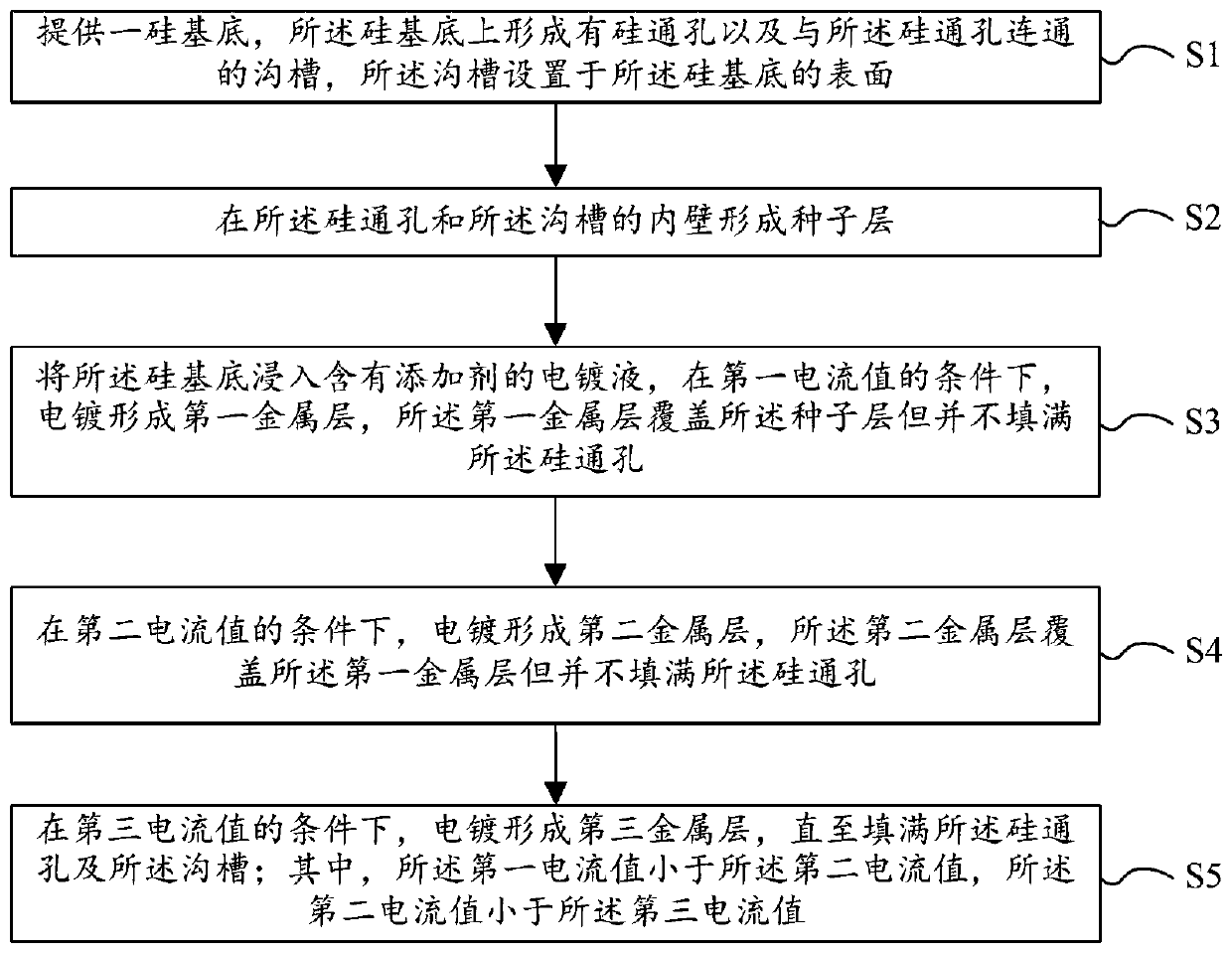
[0031] This embodiment provides a TSV electroplating method, which divides the electropla...


PUM

PropertyMeasurementUnit
pore sizeaaaaaaaaaa
thicknessaaaaaaaaaa

Abstract

The invention provides a TSV electroplating method, adding additives in the electroplating solution, electroplating the through-silicon holes on the silicon substrate and the grooves connected with them, and dividing the electroplating process into three stages by adjusting the electroplating current, three stages The electroplating currents are respectively the first current value, the second current value and the third current value, wherein the first current value is smaller than the second current value, and the second current value is smaller than the third current value, by As the plating current changes, the metal deposition rate in the through-silicon holes and the trenches connected to them changes, and eventually the through-silicon holes and trenches are filled, and no pits corresponding to the through-silicon holes are formed on the top of the electroplated metal. After removing the overplating layer above the surface of the silicon substrate, a TSV structure with a flat surface can be obtained.

Description

technical field [0001] The invention relates to an electroplating process, in particular to a TSV electroplating method. Background technique [0002] With the continuous advancement of microelectronics technology, the feature size of integrated circuits has been continuously reduced, and the interconnection density has been continuously increased. At the same time, users' requirements for high performance and low power consumption have been continuously increased. In this case, the method of improving performance by further reducing the line width of the interconnection line is limited by the physical characteristics of the material and the equipment process, and the RC (resistor-capacitance) delay of the two-dimensional interconnection line has gradually become a limit to the improvement of the performance of the semiconductor chip. the bottleneck. The TSV (Through Silicon Via) process can realize direct three-dimensional interconnection between wafers (chips) or between ...

Claims


Application Information

Patent Timeline
Patent Type & Authority Patents(China)
IPC IPC(8): C25D7/12C25D5/10C25D3/38
Inventor 龙俊舟王鹏陈红闯
Owner WUHAN XINXIN SEMICON MFG CO LTD
Why Eureka
Try Eureka