Two-dimensional array collimator with micro interval and high density and preparation method thereof

A collimator and micro-pitch technology, applied in the field of optical communication, can solve the problems of high raw material cost, large device size, and high energy consumption, and achieve the effects of high interval control accuracy, overcoming large size, and low raw material cost.

Inactive Publication Date: 2018-04-10
GUANGXUN SCI & TECH WUHAN
View PDF7 Cites 2 Cited by
  • Summary
  • Abstract
  • Description
  • Claims
  • Application Information

AI Technical Summary

Problems solved by technology

The traditional optical device assembly and combination scheme is used to achieve integration, the device size is large, the energy consumption is high, and multiple splicing leads to poor long-term use stability of the device, and the cost of manpower and material resources is very high; the integration solution realized by silicon-based chip technology, the device size It is extremely small and has high structural stability. However, due to its high technical requirements, it is still far away from commercialization; the collimator is a basic device in optical communication and is widely used in optical switches, optical isolators, and optical rings. In devices and optical dense wavelength division multiplexers, the array collimated beams formed by the array collimator are used to inject and receive optical signals in batches, and only a device core with a slightly larger size is inserted, which is packaged with the array collimator , which can make the device achieve several 10 times higher integration. This kind of integration technology is mature, the device has high stability, low cost and small size;
[0003] At present, the existing array collimator technical solutions are divided into the following types: collimator splicing scheme, using multiple individual collimators packaged in a glass plate in a certain arrangement structure to form a one-dimensional collimator array, which is limited by the size of the components Limitations, this kind of scheme has large collimator spacing and unstable packaging state, which requires more manpower and material costs; one-dimensional fiber array and lens array scheme: use one-dimensional fiber array and one-dimensional lens array to achieve packaging through a certain structural process , the formed one-dimensional array collimator has stable packaging state and high spacing density, but limited to coupling packaging technology, only one-dimensional low-density integration can be realized; two-dimensional array optical fiber and two-dimensional array lens scheme: adopt high-precision two-dimensional The two-dimensional fiber array and the two-dimensional array lens are directly coupled and packaged to form a two-dimensional array collimator, which has a high degree of integration and a simple and stable structure. However, in order to ensure that the overall insertion loss is less than 1.0dB, the positioning accuracy of the two-dimensional fiber array and the two-dimensional lens array requires Less than 0.5um, the cost of raw materials is extremely high, and it is difficult to commercialize; the solution of two-dimensional optical fiber and two-dimensional lens array with a two-dimensional correction unit: after direct coupling and packaging of a lower-precision two-dimensional optical fiber array and a two-dimensional lens array, the output At the end, a two-dimensional correction unit is used to correct the parallelism of each beam, and finally a two-dimensional collimator beam array with a higher parallelism is formed. The cost of this solution is low, but the size of the correction unit is large, and the distance between the collimators cannot be too small , and the stability of multiple correction units individually packaged devices is poor
[0004] In order to realize the extremely fine-pitch array collimator, a high-density optical fiber array and high-density lens array coupling package solution is adopted. This solution has extremely high requirements for the spacing control accuracy of the optical fiber array and lens array units, and the cost of raw materials is high; the mirror group is used to adjust The light output scheme of the collimator, the adjusted light output of the collimator is greatly affected by the angle and position of the mirror debugging package, which requires high packaging technology, or the stability of the device after packaging is poor. The cost of the film is high; the scheme of reducing the light output interval of the collimator by using the prism group also has the problem that the packaging angle and position of the prism group have a great influence on the light output of the collimator, and the requirements for debugging the packaging process are high, and the yield rate and stability Poor sex

Method used


Image

  • Two-dimensional array collimator with micro interval and high density and preparation method thereof
  • Two-dimensional array collimator with micro interval and high density and preparation method thereof
  • Two-dimensional array collimator with micro interval and high density and preparation method thereof

Examples


Embodiment 1

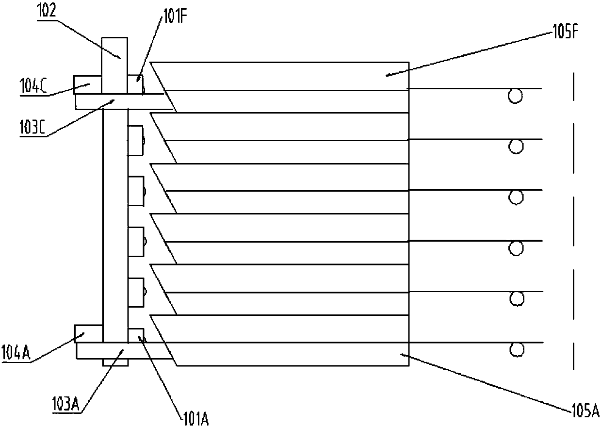
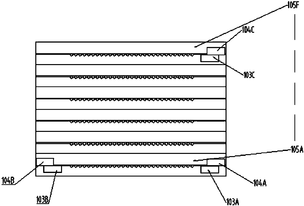
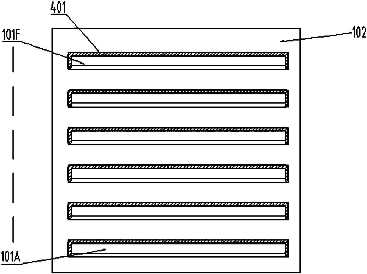
[0058] figure 1 It is the structural diagram of the array collimator of embodiment 1, figure 2 It is the layout diagram of the fixed block of the lens array frame in Embodiment 1, image 3 is the structure diagram of the lens array on the exit surface of the array collimator, Figure 4 is the focal length consistency debugging diagram of the optical fiber array, Figure 5 It is a schematic diagram of the linear misalignment of the one-dimensional lens array relative to the one-dimensional fiber array, Image 6 It is a schematic diagram of the misalignment of the center of the one-dimensional lens array relative to the one-dimensional fiber array, Figure 7 It is the lens array linearity and center alignment debugging diagram. In this embodiment, the array collimator includes: N 1×NV grooved fiber arrays 105A-105F, 3 sets of lens array frame fixing blocks 103A, 103B, 103C, 104A, 104B , 104C, a lens array fixing frame 102, and N 1×N lens arrays 101A˜101F. Wherein the 1×N f...

Embodiment 2

[0070] Figure 8It is a structural diagram of the array collimator in Embodiment 2. The array collimator in this embodiment includes: N 1×N V-groove fiber arrays 105A-105F, and three sets of lens array frame fixing blocks 103A, 103B, 103C, 104A, 104B , 104C, 1 lens array fixing frame 102, N 1×N lens arrays 101A-101F, N-1 total reflection prism strips 801A-801E, N-3 total reflection prism spacers 802A-802C. Wherein each of the 1×N fiber arrays 105A-105F is adjusted for focal length consistency and then sequentially stacked and packaged to form the N×N fiber array. One end of the lens array frame fixing block group 103A, 103B, 103C, 104A, 104B, 104C is attached to the front face of the optical fiber array, and the other end is attached to the lens array fixing frame 102, so as to realize the connection between the N×N optical fiber array and the The connection of the lens array fixing frame 102 is fixed. The 1×N lens arrays 101 are aligned with the configured 1×N optical fiber...

Embodiment 3

[0085] Figure 9 It is the structural diagram of the array collimator of embodiment 3, Figure 10 It is the structural diagram of the optical fiber array in Embodiment 3. In this embodiment, the array collimator includes: N 1×N V-groove arrays 903A-903F, N×N optical fibers 905, a fiber array cover plate 904, and a right-angle glass body 901, N fixed glass blocks 902 and N lens arrays 101A-101F. Wherein the N 1×N V-shaped grooves are laminated and bonded layer by layer after penetrating the N optical fibers, and the fiber array cover plate 904 is laminated and bonded on the top layer, and the N× N fiber array as a whole. The right-angled glass body 901 is glued to the bottom of the whole N×N optical fiber array. After the 1×N lens arrays 101 are in the debugging state, they are bonded and fixed with the fixed glass block 902 protruding from the step surface of the right-angled glass body 901, and repeated N times to form the N×N lens array in Example 3 layer by layer. Array...


PUM

PropertyMeasurementUnit
Thicknessaaaaaaaaaa
Straightnessaaaaaaaaaa

Abstract

The invention relates to a collimator and a preparation method, belongs to the technical field of optical communication, and is in particular relates to a two-dimensional array collimator based on a total reflection prism and a preparation method of the two-dimensional array collimator. Optical fiber arrays of all layers are stacked and bonded to form an optical fiber array body after the focal length of each layer of the optical fiber arrays is consistent with the focal length of each layer of the lens array, and then the uniformity index of the line degree of each layer of the lens array relative to each layer of the optical fiber array is adjusted, and each layer of the optical fiber array is independently packaged on a lens array fixing frame to form an optical fiber array front body.A one-dimensional standard array collimator is aligned with the middle layer debugging line degree and the center of an array collimator front body and then is fixed after moving the interval. The total reflection prism is packaged and fixed to the emergent end of the optical fiber array front body after being aligned with the debugging line degree and the center of the standard array collimator,so as to form a two-dimensional collimator array with extremely high interval density. The two-dimensional array collimator has the advantages that the cost of raw materials is low, and the debuggingand packaging process is easy to realize. A two-dimensional collimator array with extremely high integration level can be realized (the minimum distance is 125*250 mm<2>. ). The two-dimensional arraycollimator has the characteristics of being high in collimation parallelism, high in light spot consistency, low in insertion loss, stable in structure and the like.

Description

technical field [0001] The invention relates to a collimator and a preparation method, belonging to the technical field of optical communication, in particular to a two-dimensional micro-pitch array collimator and a preparation method. Background technique [0002] Due to the continuous and rapid development of the Internet, the communication capacity of optical networks continues to increase, and the requirements for the integration density of optical devices are getting higher and higher. The traditional optical device assembly and combination scheme is used to achieve integration, the device size is large, the energy consumption is high, and multiple splicing leads to poor long-term use stability of the device, and the cost of manpower and material resources is very high; the integration solution realized by silicon-based chip technology, the device size It is extremely small and has high structural stability. However, due to its high technical requirements, it is still f...

Claims


Application Information

Patent Timeline
IPC IPC(8): G02B27/30G02B6/32G02B6/34
CPCG02B6/32G02B6/34G02B27/30
Inventor 马雨虹杨睿袁志林宋丽丹
Owner GUANGXUN SCI & TECH WUHAN
Why Eureka
Try Eureka