Forming method of semiconductor device

A semiconductor and device technology, applied in the field of semiconductor device formation, can solve problems such as the need to improve electrical performance

Active Publication Date: 2018-04-17
SEMICON MFG INT (SHANGHAI) CORP +1
View PDF9 Cites 6 Cited by
  • Summary
  • Abstract
  • Description
  • Claims
  • Application Information

AI Technical Summary

Problems solved by technology

[0004] However, the electrical performance of semiconductor devices formed

Method used


Image

  • Forming method of semiconductor device
  • Forming method of semiconductor device
  • Forming method of semiconductor device

Examples


Embodiment Construction

[0023] As mentioned in the background, the performance of semiconductor devices formed in the prior art needs to be improved.

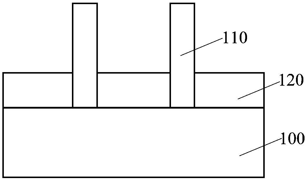
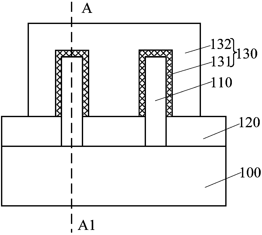
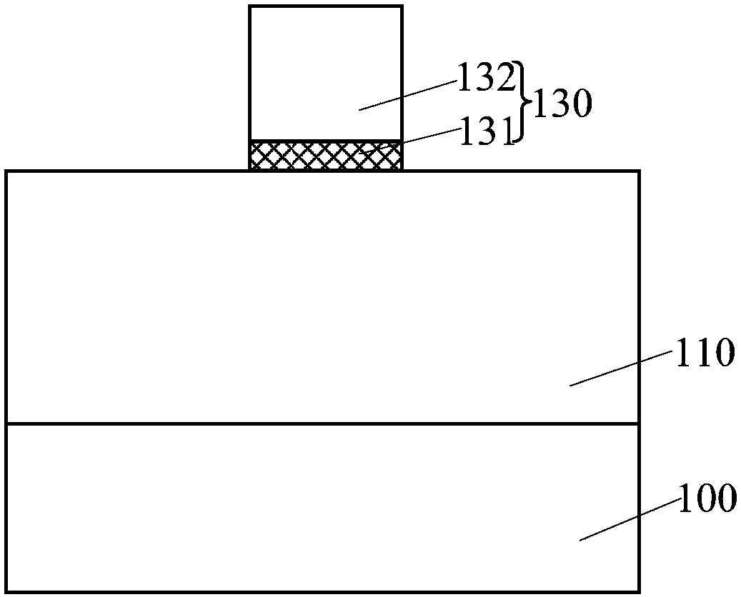
[0024] A method for forming a semiconductor device, comprising: providing a semiconductor substrate, the semiconductor substrate having a fin and an isolation structure covering part of the sidewall of the fin; forming a dummy gate across the fin on the isolation structure structure, the dummy gate structure includes a dummy gate dielectric layer and a dummy gate electrode layer, the dummy gate dielectric layer covers part of the top surface and sidewall surface of the fin, and the dummy gate electrode layer is located between the dummy gate dielectric layer and part of the On the isolation structure; forming an interlayer dielectric layer covering the sidewall of the dummy gate structure on the isolation structure; after forming the interlayer dielectric layer, removing the dummy gate electrode layer; after removing the dummy gate electrode layer, etc...


PUM

PropertyMeasurementUnit
Thicknessaaaaaaaaaa

Abstract

The invention discloses a forming method of a semiconductor device, and the method comprises the steps: providing a semiconductor substrate which is provided with a fin part and an isolation structure, wherein the isolation structure covers a part of side walls of the fin part; forming a first pseudo-gate structure across the fin part on the isolation structure, wherein the first pseudo-gate structure comprises a first pseudo-gate medium layer and first pseudo-gate electrode layers, the first pseudo-gate medium layer covers a part of the top surface and a part of side wall surfaces of the finpart, and the first pseudo-gate electrode layers are located on the first pseudo-gate medium layer and a part of isolation structure; forming interlayer medium layers on the isolation structure and the fin part, wherein the interlayer medium layers cover a part of side walls of the first pseudo-gate structure; removing the first pseudo-gate electrode layers, and forming an opening; carrying out the doping of modified ions in the isolation structure at the bottom of the opening, and forming a modified layer in the isolation structure, wherein the modified structure is aligned with the surface of the modified layer; and removing the first pseudo-gate medium layer through etching. The method can reduce the loss of the isolation structure, enables the isolation performances of the isolation structure and the modified layer for the fin part to be improved, and meets the demands of the technological design.

Description

technical field [0001] The invention relates to the field of semiconductor manufacturing, in particular to a method for forming a semiconductor device. Background technique [0002] MOS (Metal-Oxide-Semiconductor) transistors are one of the most important components in modern integrated circuits. The basic structure of the MOS transistor includes: a semiconductor substrate; a gate structure located on the surface of the semiconductor substrate, and the gate structure includes: a gate dielectric layer located on the surface of the semiconductor substrate and a gate electrode layer located on the surface of the gate dielectric layer; The source and drain doped regions in the semiconductor substrate on both sides of the pole structure. [0003] With the development of semiconductor technology, the ability of the traditional planar MOS transistor to control the channel current becomes weaker, resulting in serious leakage current. Fin Field Effect Transistor (Fin FET) is an eme...

Claims


Application Information

Patent Timeline
IPC IPC(8): H01L21/8234H01L21/336
CPCH01L21/823431H01L29/66795
Inventor 周飞
Owner SEMICON MFG INT (SHANGHAI) CORP
Why Eureka
Try Eureka