CMOS single-photon avalanche diode specific to long-wave-band weak light

A single-photon avalanche, weak light technology, applied in the field of photoelectric detection, can solve the problems of large dark count rate noise, restricting the development of detectors, etc.

Inactive Publication Date: 2018-04-20
CHONGQING UNIV OF POSTS & TELECOMM
View PDF5 Cites 21 Cited by
  • Summary
  • Abstract
  • Description
  • Claims
  • Application Information

AI Technical Summary

Problems solved by technology

Although the STI guard ring has a relatively high fill factor, due to the direct contact between the active region of the APD and the STI, free carriers enter the sensitive region of the detector, resulting in a large noise in the dark count rate, which seriously restricts the detection of weak light by the detector. field development

Method used


Image

  • CMOS single-photon avalanche diode specific to long-wave-band weak light
  • CMOS single-photon avalanche diode specific to long-wave-band weak light
  • CMOS single-photon avalanche diode specific to long-wave-band weak light

Examples


Embodiment Construction

[0023] The technical solutions in the embodiments of the present invention will be described clearly and in detail below with reference to the drawings in the embodiments of the present invention. The described embodiments are only some of the embodiments of the invention.

[0024] The technical scheme that the present invention solves the problems of the technologies described above is:

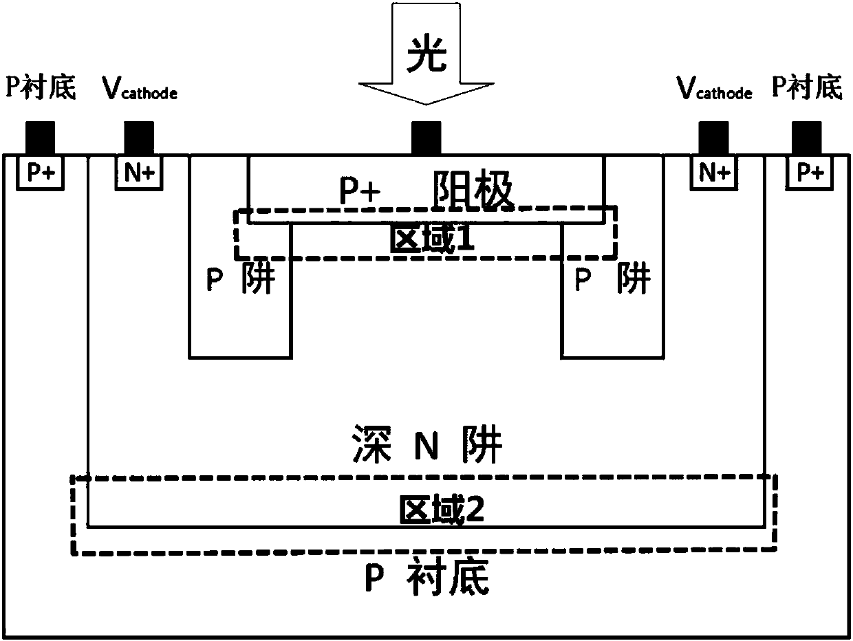
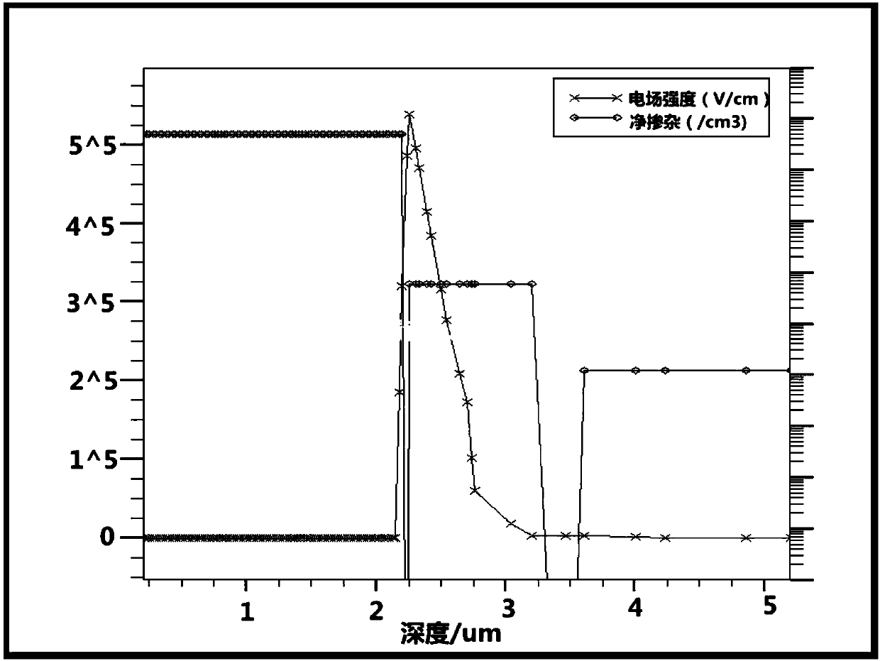
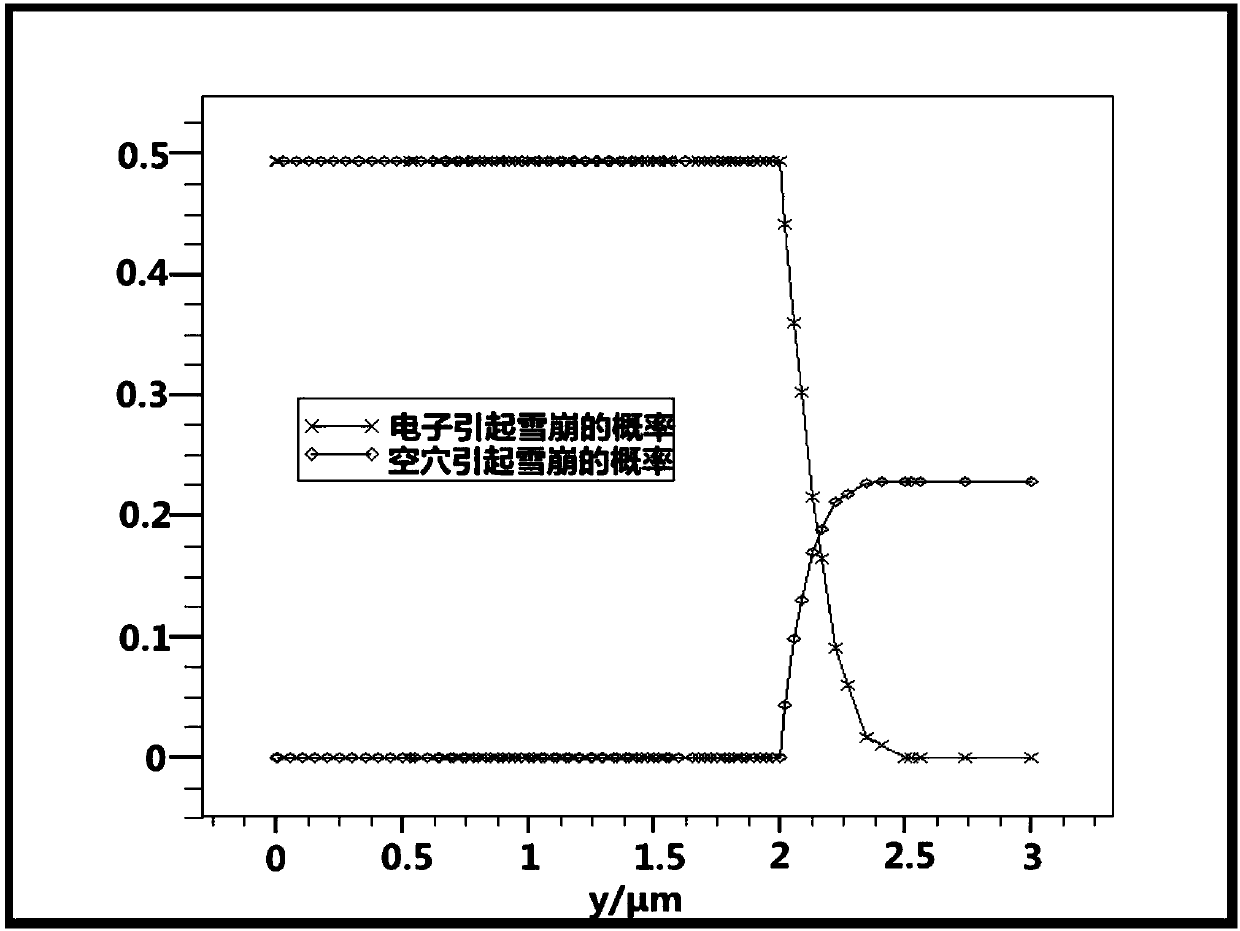
[0025] This paper proposes a PN-type single-photon avalanche diode (SPAD) structure based on CMOS process technology. This structure SPAD has obvious advantages in responsivity and detection efficiency, and can achieve good detection of weak light signals in the near-infrared band. Traditional CMOS SPADs use shallow P+ / N well junctions, and their spectral responsivity peaks are mainly concentrated in the blue-green light region, while the detection sensitivity to long-wavelength light is not ideal. In this paper, a P+ / deep N well dual diode structure is proposed, which can effectively solve...


PUM


Abstract

The invention provides a CMOS single-photon avalanche diode specific to long-wave-band weak light. According to the specific structure, a deep N well is manufactured on a P type substrate; next, a P type heavily doped region is manufactured in the deep N well; a PN junction is formed by a P+ layer and the deep N well to be used as an avalanche multiplication region; the P+ region is surrounded bya lightly doped P well to be used as a protection ring; and after incident light comes to a device, the deep N well region in a medium electric field strength is absorbed, and the generated photon-generated carriers move towards an avalanche multiplication region of a strong electric field region. Electron holes generated by light of relatively long waveband are formed in a relatively deep position of the device, so that the light signals can be detected effectively by the deep N well; by taking the deep N well / P substrate as a shielding diode, diffusion of the substrate photon-generated carriers to the PN junction can be prevented, thereby reducing influence of diffusion of substrate slow photon-generated carriers to the response speed of a photoelectric detector; and the absorption efficiency of the device in a long waveband can be improved.

Description

technical field [0001] The invention belongs to the technical field of photoelectric detection and relates to the structure of photoelectric devices, in particular to the design of a CMOS SPAD photoelectric device with high detection efficiency for long-wave weak light. Background technique [0002] Long-wavelength light can reduce cell damage and penetrate deeper into tissues. Therefore, research on improving the sensitivity of detectors in the infrared and near-infrared bands is of great significance in improving the quality of bioluminescent lifetime imaging and optical tomography. [0003] Avalanche photodiode (Avalanche Photodiode, APD) is a solid-state photoconductive device with a p-n junction operating under reverse bias. The principle of avalanche multiplication is: the incident light is absorbed in the depletion region of the reverse-biased p-n junction, and converted into electron-hole pairs. These primary electron-hole pairs drift under the action of a strong ele...

Claims


Application Information

Patent Timeline
Patent Type & Authority Applications(China)
IPC IPC(8): H01L31/0352H01L31/107H01L31/18
CPCH01L31/035272H01L31/03529H01L31/107H01L31/1876Y02P70/50
Inventor 王巍陈婷李俊峰杨皓徐媛媛李双巧王广王冠宇袁军杨正琳
Owner CHONGQING UNIV OF POSTS & TELECOMM
Why Eureka
Try Eureka