

Layered-structure asymmetric MXene and derived heterojunction thereof
A layered, asymmetric technology, applied in electrical components, circuits, semiconductor devices, etc., to solve problems such as limited heterojunctions
- Summary
- Abstract
- Description
- Claims
- Application Information
AI Technical Summary
Problems solved by technology
Method used
Image

Examples
Embodiment
[0034] The first-principle calculations used in this embodiment are all performed by VASP (Vienna Ab initio Simulation Package). The plane wave cut-off energy is set to 450eV, and the convergence accuracy standard for the force of each atom is set to The PBE method and the HSE06 method both choose the Monkhorst-Pack method for the K-point sampling method in the inverted space, and the K-point sampling grids are 15×15×1 and 7×7×1 respectively. Interface binding energy [interfacial bindingenergy(E b )] by the formula E b =E aMXene +E mTMDC -E hetero Calculated, E hetero ,E mTMDC and E aMXene Denote the total energy of the heterostructure, mTMDC and aMXene, respectively.
[0035] In this embodiment, M is one of Sc, V, Ti or Cr, M' is Mo or W, T is O, and X is S or Se.
[0036] 1. Geometric structure of aMXene and its strong built-in electric field
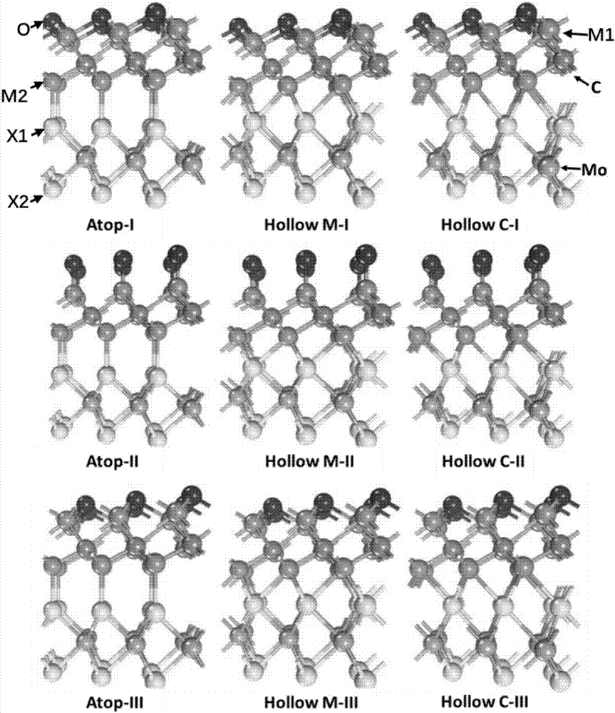
[0037] In this example, the configuration of aMXene is first considered. For single-layer metal carbide M-C-M (M=Sc, V, ...
PUM
 Abstract
Description
Claims
Application Information