Conductive-particle-free electromagnetic shielding film and preparation method thereof
An electromagnetic shielding film, non-conductive technology, applied in the direction of magnetic/electric field shielding, electrical components, etc., can solve the problems of complex process operation and large thickness, and achieve the effect of simple process, thin thickness, and reduced overall thickness
- Summary
- Abstract
- Description
- Claims
- Application Information
AI Technical Summary
Problems solved by technology
Method used
Image
Examples
Embodiment 1
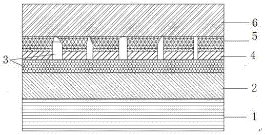
[0040] Embodiment 1: A structure of electromagnetic shielding film without conductive particles
[0041] structured as figure 1 , figure 2 , image 3 As shown, from bottom to top are carrier film (1), insulating layer (2), shielding layer (3), covering layer (4), adhesive layer (5), protective film (6); the covering Holes of different sizes are distributed on the surface of the layer (4); the shielding layer (3) is composed of a plane metal (31) and a convex metal (32), wherein the plane metal (31) is compounded on the insulating layer (2), and the convex The shape metal (32) is distributed in the holes (4) of the covering layer and is in contact with the plane metal (31).
Embodiment 2
[0042] Embodiment 2: An electromagnetic shielding film without conductive particles
[0043] Structure is as described in embodiment 1;
[0044] The dimensions are: the thickness of the carrier film (1) is 25 μm; the thickness of the insulating layer (2) is 6 μm; the thickness of the cover layer (4) is 0.1 μm; the thickness of the bonding layer (5) is 1 μm; the thickness of the protective film (6) is 150 μm; The thickness of the flat metal (31) is 0.1 μm; the height of the convex metal (32) is 5 μm; the hole diameter is 1-10 μm;
[0045] The material is: the carrier film is a PET film;
[0046] The insulating layer is composed of polymer material and silicon dioxide in a mass ratio of 1:1, and the polymer material is composed of epoxy resin and rubber in a mass ratio of 1:1;
[0047] The plane metal is copper, nickel alloy; the convex metal is copper;
[0048] The covering layer is composed of high molecular polymer and silicon surfactant in a mass ratio of 1:0.001; the hig...
Embodiment 3
[0056] Embodiment 3: An electromagnetic shielding film without conductive particles
[0057] Structure is identical with embodiment 1;
[0058] The dimensions are: the thickness of the carrier film (1) is 150 μm; the thickness of the insulating layer (2) is 5 μm; the thickness of the cover layer (4) is 0.5 μm; the thickness of the adhesive layer (5) is 2 μm; the thickness of the protective film (6) is 50 μm; The thickness of the plane metal (31) is 0.5 μm; the height of the convex metal (32) is 5 μm; the hole diameter is 40-50 μm;
[0059] The material is: the carrier film is a PI film;
[0060] The insulating layer is composed of polymer material and functional filler in a mass ratio of 5:1; the polymer material is composed of polyimide resin and polyurethane resin in a mass ratio of 2:1, and the functional filler is composed of silicon dioxide and aluminum nitride in a mass ratio of 2:1. Composition with a mass ratio of 1:1;
[0061] The plane metal is copper; the convex ...
PUM
| Property | Measurement | Unit |
|---|---|---|
| thickness | aaaaa | aaaaa |
| thickness | aaaaa | aaaaa |
| thickness | aaaaa | aaaaa |
Abstract
Description
Claims
Application Information
 - R&D
- Intellectual Property
- Life Sciences
- Materials
- Tech Scout
- Unparalleled Data Quality
- Higher Quality Content
- 60% Fewer Hallucinations
Browse by: Latest US Patents, China's latest patents, Technical Efficacy Thesaurus, Application Domain, Technology Topic, Popular Technical Reports.
© 2025 PatSnap. All rights reserved.Legal|Privacy policy|Modern Slavery Act Transparency Statement|Sitemap|About US| Contact US: help@patsnap.com


