TFT (thin-film transistor) substrate and manufacture method thereof

A manufacturing method and substrate technology, applied in semiconductor/solid-state device manufacturing, electrical components, electrical solid-state devices, etc., can solve the problems of difficult process adjustment, difficult performance guarantee, and TFT device difficulty, so as to reduce costs, improve performance, The effect of simplifying the preparation process

Active Publication Date: 2018-05-04
SHENZHEN CHINA STAR OPTOELECTRONICS SEMICON DISPLAY TECH CO LTD
View PDF10 Cites 1 Cited by
  • Summary
  • Abstract
  • Description
  • Claims
  • Application Information

AI Technical Summary

Problems solved by technology

However, this method is difficult to adjust the process and performance is difficult to guarantee, and it is difficult to apply to TFT devices in the display industry

Method used


Image

  • TFT (thin-film transistor) substrate and manufacture method thereof
  • TFT (thin-film transistor) substrate and manufacture method thereof
  • TFT (thin-film transistor) substrate and manufacture method thereof

Examples


Embodiment Construction

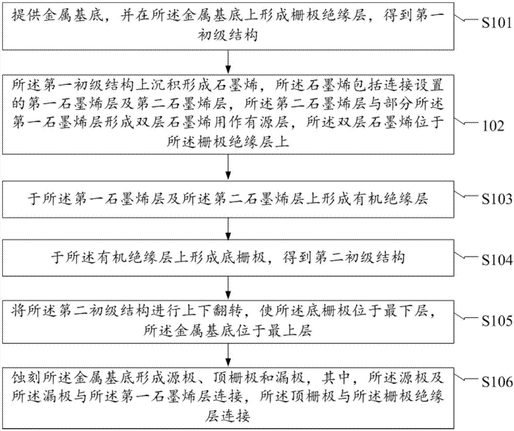
[0041] The following will clearly and completely describe the technical solutions in the embodiments of the present invention with reference to the accompanying drawings in the embodiments of the present invention. Obviously, the described embodiments are only some, not all, embodiments of the present invention. Based on the embodiments of the present invention, all other embodiments obtained by persons of ordinary skill in the art without creative efforts fall within the protection scope of the present invention.

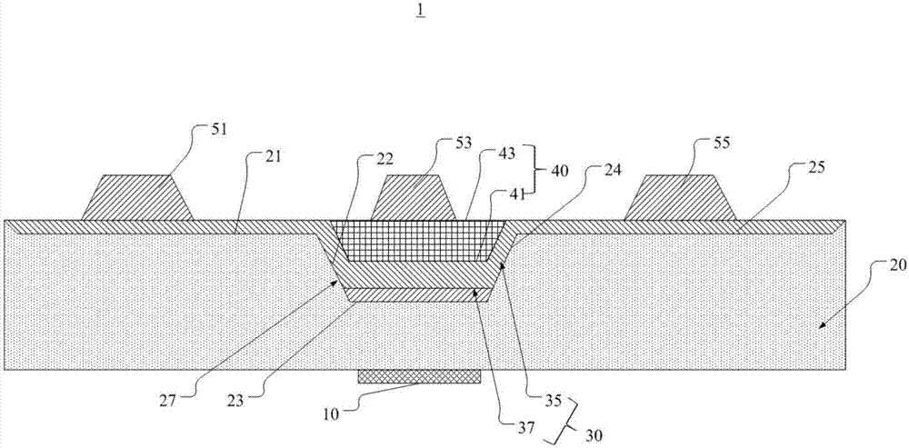
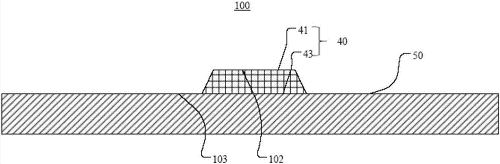
[0042] see figure 1 , is a TFT substrate 1 provided by an embodiment of the present invention. The TFT substrate 1 includes a bottom gate 10 , an organic insulating layer 20 , graphene 30 , a gate insulating layer 40 , a source 51 , a top gate 53 and a drain 55 .

[0043] Specifically, in this embodiment, the bottom gate 10 is a carbon nanotube layer. It can be understood that the bottom gate 10 can also be one of molybdenum (Mo), aluminum (Al), and copper (Cu). ...


PUM

PropertyMeasurementUnit
thicknessaaaaaaaaaa

Abstract

A manufacture method of a TFT (thin-film transistor) substrate comprises: providing a metal substrate, and forming a gate insulating layer on the metal substrate to obtain a first primary structure; depositing on the first primary structure to obtain graphene that includes a first graphene layer and a second graphene layer which are connected, wherein the second graphene layer and part of the first graphene layer form double graphene layers to serves as an active layer, and the double graphene layers are positioned on the gate insulating layer; forming an organic insulating layer on graphene;forming a bottom gate on the organic insulating layer to obtain a second primary structure; flipping the second primary structure so that the bottom gate is positioned as a lowermost layer and the metal substrate as an uppermost layer; etching the metal substrate to form a source, a top gate and a drain, wherein the source and the drain are connected with the first graphene layer, and contact resistance between the source and drain and the double graphene layers is decreased. The invention also provides a TFT substrate.

Description

technical field [0001] The invention relates to the field of display technology, in particular to a TFT substrate and a manufacturing method thereof. Background technique [0002] In the active matrix display technology, each pixel is driven by a Thin Film Transistor (TFT) integrated behind it, so that high-speed, high-brightness, and high-contrast screen display effects can be achieved. A common TFT is usually composed of gate / source / drain (Gate / Source / Drain) three electrodes, an insulating layer and a semiconductor layer. [0003] Graphene, as the thinnest and hardest nanomaterial known in the world, has become one of the current research hotspots because of its good electrical conductivity, mechanical properties, and thermal conductivity. Graphene, as a new material with extremely thin and extremely high conductivity, has great potential to be applied to electronic components / transistors. According to reports, graphene films have extremely low sheet resistance (<100Ω...

Claims


Application Information

Patent Timeline
Patent Type & Authority Applications(China)
IPC IPC(8): H01L21/77H01L27/12
CPCH01L27/1218H01L27/1222H01L27/1266H01L27/127
Inventor 夏慧
Owner SHENZHEN CHINA STAR OPTOELECTRONICS SEMICON DISPLAY TECH CO LTD
Why Eureka
Try Eureka