Epitaxial structure and preparation method of high-frequency gan rectifier with n-polar surface on silicon substrate
A technology of epitaxial structures and polar planes, which is applied in semiconductor/solid-state device manufacturing, diodes, semiconductor devices, etc. Problems such as difficulty in the growth of texture junctions, to achieve the effect of increasing the two-dimensional electron gas confinement threshold, reducing the two-dimensional electron gas confinement threshold, and inhibiting the melting back etching reaction
- Summary
- Abstract
- Description
- Claims
- Application Information
AI Technical Summary
Problems solved by technology
Method used
Image
Examples
Embodiment 1
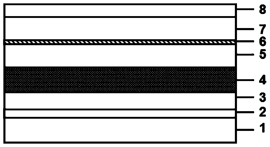
[0033] Such as figure 1As shown, the epitaxial structure of the N-polar plane high-frequency GaN rectifier on the silicon substrate of this embodiment includes the non-doped N-polar plane GaN buffer layer (including the N-polar plane GaN buffer layer) grown sequentially on the silicon substrate 1. The layer includes the non-doped N polar surface AlN buffer layer 2 and the non-doped N polar surface composition graded Al y Ga 1-y N buffer layer 3), carbon doped N polar GaN layer 4, non-doped N polar surface Al x Ga 1-x N layer 5, non-doped N-polar surface AlN insertion layer 6, non-doped N-polar surface GaN layer 7, N-polar InGaN layer 8; where x=0.3, y=0.15˜0.45.
[0034] The non-doped N-polar surface GaN buffer layer of this embodiment is 750nm, wherein the thickness of the non-doped N-polar surface AlN buffer layer is 150nm, and the non-doped N-polar surface composition is graded Al y Ga 1-y N (from bottom to top y=0.35, 0.18) buffer layer thickness is 650nm; the carbon-...
Embodiment 2
[0047] The preparation method of the high-frequency GaN rectifier epitaxial structure on the N-polar plane on the silicon substrate of this embodiment is as follows:
[0048] (1) Selection of the substrate and its crystal orientation: a single crystal silicon substrate is used, and the Si(111) close-packed surface is used as the epitaxial surface. The direction is used as the epitaxial growth direction of the material;
[0049] (2) Substrate surface cleaning: Put the silicon substrate into acetone, absolute ethanol, and deionized water in sequence, and ultrasonically clean it for 5 minutes in sequence. After taking it out, rinse it with deionized water and dry it with hot high-purity nitrogen;
[0050] (3) Epitaxial growth of the AlN buffer layer on the non-doped N polar surface: using the pulsed laser deposition process, put the clean substrate into the vacuum chamber, raise the substrate temperature to 420°C, and pump the vacuum in the chamber to 2.0× 10 -4 torr, the lase...
Embodiment 3
[0060] (1) Selection of the substrate and its crystal orientation: a single crystal silicon substrate is used, and the Si(111) close-packed surface is used as the epitaxial surface. The direction is used as the epitaxial growth direction of the material;
[0061] (2) Substrate surface cleaning: Put the silicon substrate into acetone, absolute ethanol, and deionized water in sequence, and ultrasonically clean it for 15 minutes in sequence. After taking it out, rinse it with deionized water and dry it with hot high-purity nitrogen;
[0062] (3) Epitaxial growth of the AlN buffer layer on the non-doped N polar surface: using the pulsed laser deposition process, put the clean substrate into the vacuum chamber, raise the substrate temperature to 500°C, and pump the vacuum to 4.0× 10 -4 torr, the laser energy is 320mJ, the laser frequency is 0Hz, the nitrogen flow rate is 10sccm, and the N-polar AlN film is grown under N-rich conditions, and the Al source is AlN high-purity cerami...
PUM
 Abstract
Description
Claims
Application Information


