p-GaN gate enhanced GaN-HEMT device capable of reducing gate electric leakage and manufacturing method thereof
An enhanced, p-gan technology used in microelectronics to address issues such as gate degradation
- Summary
- Abstract
- Description
- Claims
- Application Information
AI Technical Summary
Problems solved by technology
Method used
Image
Examples
Embodiment 1
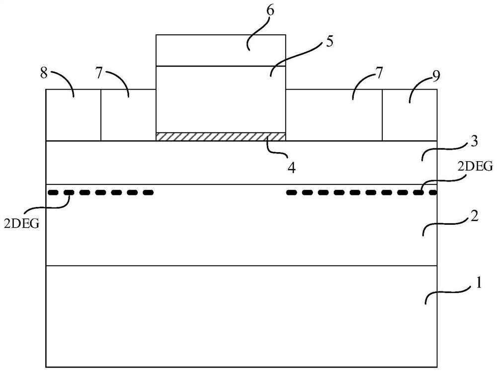
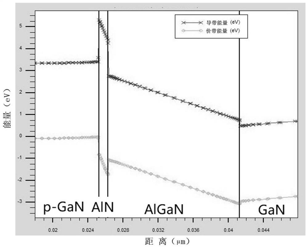
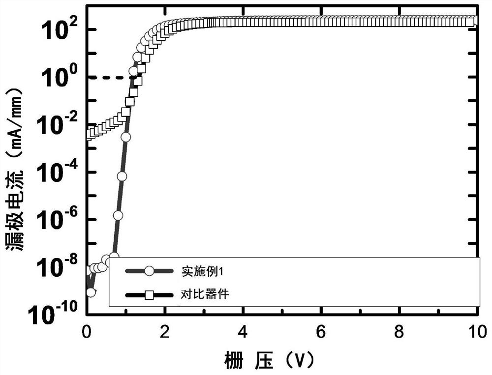
[0031] The p-GaN gate-enhanced GaN-HEMT device with reduced gate leakage provided by the invention of this embodiment, such as figure 1 As shown, it includes a substrate 1, a GaN buffer layer 2 and an AlGaN barrier layer 3 arranged from bottom to top, and the AlGaN barrier layer 3 is provided with an AlN high barrier layer 4, a p-GaN layer 5 and a gate A gate structure composed of pole 6; a source 8 and a drain 9 are arranged on the AlGN barrier layer on both sides of the gate structure; the AlGN barrier layer between the gate and the source, and between the gate and the drain A passivation layer 7 is provided thereon. In this embodiment, the gate p-GaN / AlN / AlGaN / GaN forms a p-i-n junction, which consumes the two-dimensional electron gas in the AlGaN / GaN channel under the gate, so that the device is in an off state at zero gate voltage, realizing an enhanced mode. Such a structure can make the device need to apply a positive gate voltage greater than the threshold voltage. Af...
Embodiment 2
[0041] This embodiment provides a method for manufacturing a p-GaN gate-enhanced GaN-HEMT device with reduced gate leakage in Embodiment 1, including the following steps:
[0042] S1 uses MOCVD epitaxial growth technology to epitaxially grow a GaN buffer layer, an AlGaN barrier layer, an AlN high barrier layer and a p-GaN layer on a silicon substrate in sequence to form a p-GaN / AlN / AlGaN / GaN heterojunction structure;
[0043] S2 Perform photolithography and dry ICP dry etching on the p-GaN / AlN / AlGaN / GaN epitaxial material to form active region mesas;
[0044] S3 On the basis of step S2, perform photolithography on the p-GaN / AlN / AlGaN / GaN epitaxial wafer with prepared mesas, retain the gate area, and then use ICP dry etching technology to vertically remove the p-GaN outside the gate area layer and AlN high barrier layer;
[0045] S4 On the basis of step S3, perform photolithography on the device to form the source and drain areas to be evaporated, and then use electron beam ev...
PUM
| Property | Measurement | Unit |
|---|---|---|
| Thickness | aaaaa | aaaaa |
| Thickness | aaaaa | aaaaa |
| Thickness | aaaaa | aaaaa |
Abstract
Description
Claims
Application Information


