
GaAs-based PMOS device manufacturing method

A manufacturing method and device technology, applied in semiconductor/solid-state device manufacturing, semiconductor devices, electrical components, etc., can solve the problems of slow progress of PMOS devices, achieve mobility and high electron concentration, low interface state density, and improve the Dimensional electron gas concentration effect

Inactive Publication Date: 2017-05-31
DONGGUAN GUANGXIN INTPROP SERVICES CO LTD +1
View PDF3 Cites 0 Cited by
  • Summary
  • Abstract
  • Description
  • Claims
  • Application Information

AI Technical Summary

Problems solved by technology

However, PMOS devices using III-V semiconductor materials as channel materials have been slow to progress

Method used


Image

  • GaAs-based PMOS device manufacturing method
  • GaAs-based PMOS device manufacturing method
  • GaAs-based PMOS device manufacturing method

Examples


Embodiment Construction

[0025] In order to make the object, technical solution and advantages of the present invention clearer, the present invention will be described in further detail below in conjunction with specific embodiments and with reference to the accompanying drawings.

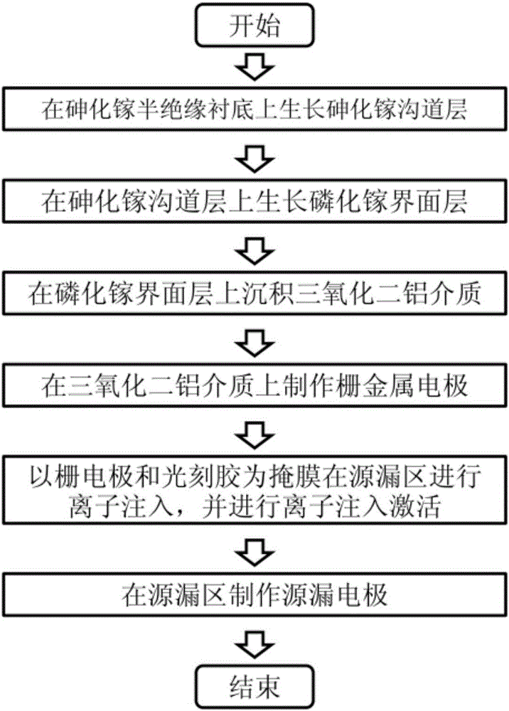
[0026] Such as Figure 2-7 as shown, Figure 2-7 This embodiment provides a method for manufacturing a gallium arsenide PMOS device.

[0027] Its production steps are as follows:

[0028] (1) if figure 2 As shown, the N-type doped gallium arsenide channel layer (102) with a doping concentration of 5×10 is grown on a semi-insulating gallium arsenide substrate (101) with a thickness of 100 nanometers. 17 cm -3 , the doping impurity is silicon;

[0029] (2) if image 3 As shown, a gallium phosphide interface layer (103) with a thickness of 1 nanometer is grown on the gallium arsenide channel layer (102);

[0030] (3) if Figure 4 As shown, a 3-nanometer-thick aluminum oxide medium (104) is grown on the surface of th...


PUM

PropertyMeasurementUnit
thicknessaaaaaaaaaa
thicknessaaaaaaaaaa
thicknessaaaaaaaaaa

Abstract

The present invention discloses a GaAs-based PMOS device manufacturing method. The manufacturing method comprises the steps: growing an N-type doped gallium arsenide channel layer (102) with the thickness of 100 nanometers on a semi-insulating gallium arsenide substrate (101); growing a gallium phoshpide interface layer (103) with the thickness of 1 nanometer on the N-type doped gallium arsenide channel layer (102); growing an aluminum oxide medium (104) with the thickness of 3 nanometers on the surface of the gallium phoshpide interface layer (103); depositing a gate metal electrode (105) on the aluminum oxide medium (104); employing a photoresist mask method to perform ion implantation at a source drain area (106), wherein the injected ion is Be; performing ion implantation activation at the source drain area; and making the source drain metal electrode platinum / titanium / gold (107) at the source drain area (106).

Description

technical field [0001] The invention relates to the technical field of manufacturing semiconductor integrated circuits, in particular to a method for manufacturing gallium arsenide PMOS devices, which is applied to high-performance III-V semiconductor CMOS technology. Background technique [0002] Compared with silicon materials, III-V compound semiconductor materials have the advantages of high carrier mobility, large forbidden band width, etc., and have good characteristics in thermal, optical and electromagnetic aspects. Over the past forty years, high-quality thermally stable gate dielectric materials and the lack of PMOS devices matching NMOS devices have been the main obstacles to the application of III-V semiconductors in large-scale CMOS integrated circuits. The latest research reports show that on the surface of III-V semiconductors, the direct use of atomic layer deposition (ALD) and molecular beam epitaxy (MBE) to deposit high-k gate dielectric materials has achie...

Claims


Application Information

Patent Timeline
Patent Type & Authority Applications(China)
IPC IPC(8): H01L21/336H01L29/78H01L29/20H01L29/06
Inventor 刘丽蓉王勇丁超
Owner DONGGUAN GUANGXIN INTPROP SERVICES CO LTD
Learn More