A method of manufacturing a semiconductor device

A manufacturing method and semiconductor technology, which is applied in the direction of semiconductor/solid-state device manufacturing, semiconductor devices, electrical components, etc., can solve the problems of target pattern distortion, poor surface roughness of spacer wall, and complicated process, so as to improve yield and performance, The effect of small process fluctuation and improved robustness

Active Publication Date: 2020-08-14
SEMICON MFG INT (SHANGHAI) CORP +1
View PDF6 Cites 0 Cited by
  • Summary
  • Abstract
  • Description
  • Claims
  • Application Information

AI Technical Summary

Problems solved by technology

The traditional quadruple pattern lithography technology also has its deficiencies, for example, it is necessary to introduce complex film layer stacks to realize the pattern transfer, which forms a spacer on the mandrel in the upper layer, and defines the mandrel in the lower layer with the spacer (mandrel), and in this process, it is necessary to ensure that the mandrel formed on the lower layer is a square pattern (square pattern)
It can be seen that the traditional process has complex processes, requires multiple depositions of film layers, high process costs, and poor surface roughness of the formed spacers.
In addition, when removing the mandrel by etching, it is easy to over-etch the oxide hard mask layer on both sides of the spacer, so that the height of the oxide on both sides of each spacer is inconsistent, resulting in subsequent etching using the spacer as a mask. When the target pattern is formed on the semiconductor substrate, the formed target pattern is distorted, the pitch deviates, and the pattern transfer quality is poor, which negatively affects the robustness of the device

Method used


Image

  • A method of manufacturing a semiconductor device
  • A method of manufacturing a semiconductor device
  • A method of manufacturing a semiconductor device

Examples


Embodiment 1

[0050] In order to solve the above technical problems, the present invention provides a method for manufacturing a semiconductor device, such as image 3 As shown, it mainly includes the following steps:

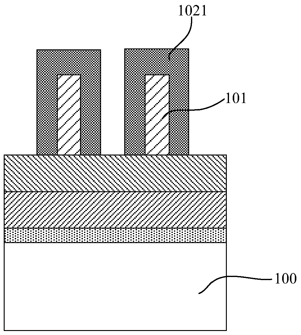
[0051] Step S301, providing a semiconductor substrate on which a target material layer is formed;

[0052] Step S302, forming a plurality of first spacers arranged at intervals on the target material layer;

[0053] Step S303, performing a first plasma treatment to modify the first spacer to form a modified first spacer;

[0054] Step S304, forming a second spacer material layer to cover the modified first spacer and part of the surface of the semiconductor substrate;

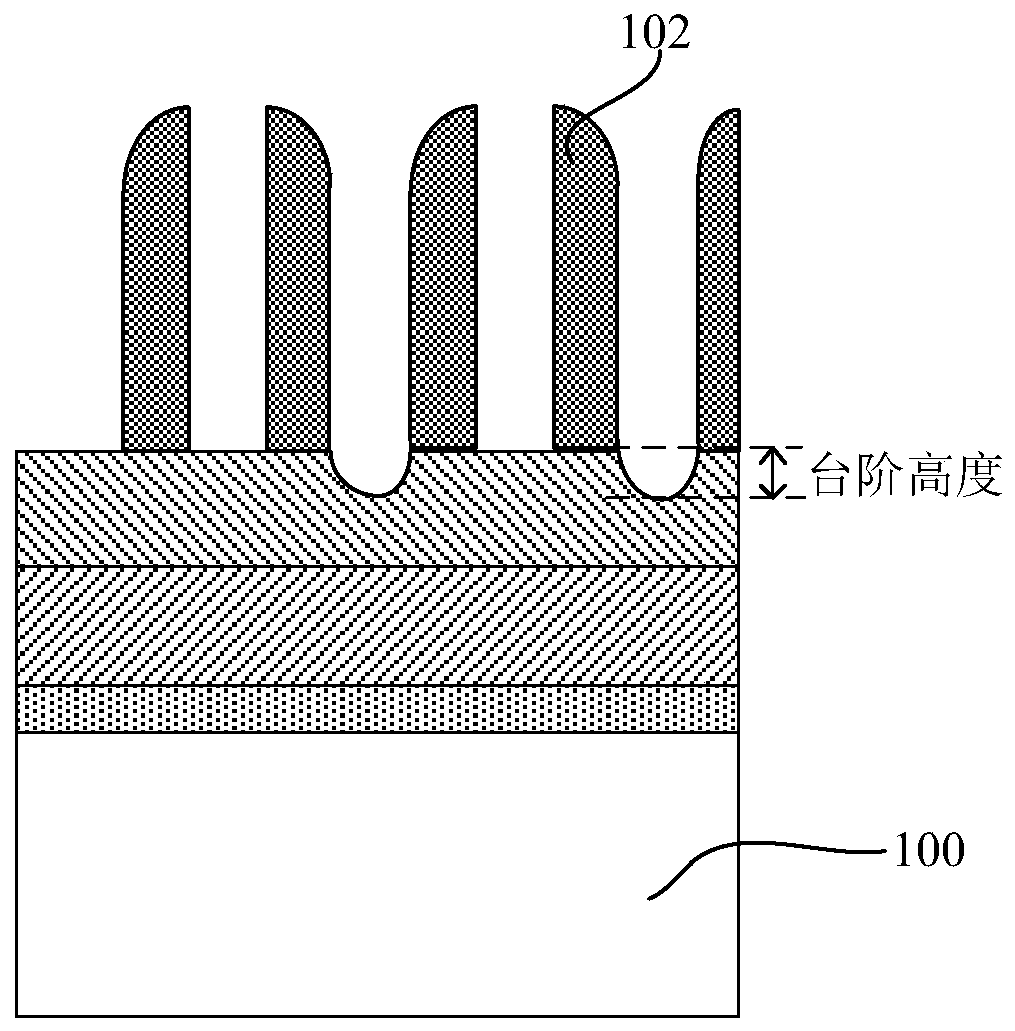
[0055] Step S305, performing a second plasma treatment to modify the portion of the second spacer material layer located on the top surface of the modified first spacer and the portion located on the surface of the target material layer, thereby forming a modified second spacer material layer;

[0056] St...


PUM


Abstract

The invention provides a manufacture method of a semiconductor device and relates to the field of semiconductor technology. The method includes provides a semiconductor substrate on which a target material layer is formed; forming a plurality of first gap walls arranged at intervals on the target material layer; performing first plasma processing so as to modify the first gap walls and thus to form the modified first gap walls; forming a second gap wall material layer for covering the modified first gap walls and a part of the surface of the target material layer; performing second plasma processing for modifying a part of the second gap wall material layer on the top face of the modified first gap walls and a part of the second gap wall material layer on the surface of the target materiallayer so as to form a modified second gap wall material layer; removing the modified first gap walls and the modified second gap wall material layer so as to form a plurality of second gap walls arranged at intervals. The manufacture method provided by the invention improves yield an performance of the device.

Description

technical field [0001] The invention relates to the technical field of semiconductors, in particular to a method for manufacturing a semiconductor device. Background technique [0002] With the increasing demand for high-capacity semiconductor storage devices, the integration density of semiconductor storage devices has attracted people's attention. In order to increase the integration density of semiconductor storage devices, many different methods have been adopted in the prior art. -Patterning, DP) is being widely accepted and applied as a solution in the fabrication of semiconductor devices. [0003] Double-patterning (DP) technology overcomes the K1 limitation through pitch fragmentation, and thus is widely used in the preparation of semiconductor devices. At present, in Double-Patterning (DP) technology, there are self-aligned double patterning (Self-aligned double patterning, SADP), lithography-etching-lithography-etch (Litho-Etch-Litho-Etch, LELE) And freeze coatin...

Claims


Application Information

Patent Timeline
Patent Type & Authority Patents(China)
IPC IPC(8): H01L29/78H01L21/336H01L21/265
CPCH01L21/265H01L29/66795H01L29/785
Inventor 张海洋王彦蒋鑫
Owner SEMICON MFG INT (SHANGHAI) CORP
Why Eureka
Try Eureka