Melt direct writing process based micro-channel chip manufacturing processing system and processing method

A processing system and micro-channel technology, applied in the field of micro-fluidic device processing system, can solve the problems of micro-fluidic chip line width limitation, time-consuming and expensive, complicated manufacturing method, etc., to improve aspect ratio, reduce Width, the effect of improving copy accuracy

Inactive Publication Date: 2018-05-15
GUANGDONG UNIV OF TECH
View PDF5 Cites 3 Cited by
  • Summary
  • Abstract
  • Description
  • Claims
  • Application Information

AI Technical Summary

Problems solved by technology

In the 1990s, the microfluidic method of using photolithography on the silicon wafer base was the most popular processing technology, and batch after batch of highly integrated microfluidic chips were produced, which were used in biological and In the field of medicine, such as DNA array [Weston M C, Gerner M D, Fritsch I. Magnetic fields for fluid motion [J]. 2010. etc.], clinical diagnosis and research of cells and proteins (Jebrail M J, Yang H, Mudrik J M, et al. al.A digital microfluidic method for dried blood spot analysis[J].Lab on a Chip,2011,11(19):3218-3224.), using the microfluidic method based on glass and silicon substrates can provide higher flow channels precision, but the manufacturing method is complicated, time-consuming and expensive
In response to this problem, some researchers used 3D printing to make the main mold, and used curing agents such as dimethylsiloxane (PDMS, etc.) Conventional processes such as lithography and etching are required, as well as special processes such as molding, soft lithography, laser ablation and LIGA technology. For polymer materials, processes such as surface modification and bonding are also required. Therefore, the current The processing technology has the disadvantages of cumbersome steps, pollution and expensive equipment
[0003] In view of the above problems, Chinese invention patent CN102411060A discloses a microfluidic chip with a high aspect ratio microfluidic channel and its manufacturing method, which realizes a high aspect ratio microfluidic chip by stacking multilayer substrates processing and manufacturing, although the method described in the invention has low technological requirements, but the method steps are complex and need to achieve multiple interleaving. In addition, the line width of the microfluidic chip based on photolithography processing is limited. It is difficult to process wide runners

Method used


Image

  • Melt direct writing process based micro-channel chip manufacturing processing system and processing method
  • Melt direct writing process based micro-channel chip manufacturing processing system and processing method
  • Melt direct writing process based micro-channel chip manufacturing processing system and processing method

Examples


Embodiment Construction

[0023] In order to make the technical problems, technical solutions and advantages to be solved by the present invention clearer, the following will describe in detail with reference to the drawings and specific embodiments.

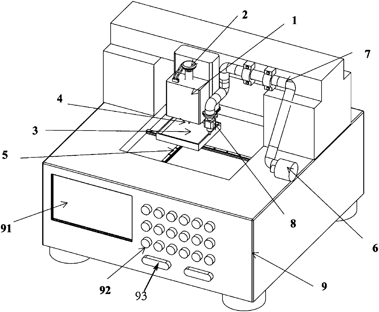
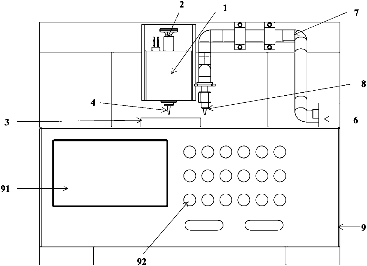
[0024] Such as figure 1 , figure 2 As shown, a processing system for fabricating microfluidic chips based on the melt direct writing process, including a melt direct writing deposition device, a curing agent liquid addition device and a control device, wherein,

[0025] Described control device comprises control box 9, is provided with microprocessor in the described control box 9, is provided with display screen 91, acquisition switch 93 and function key 92 on the casing of described control box 9, and described function key 92 and The signal input end of the microprocessor is connected, and the display screen 91 is connected with the signal output end of the microprocessor (FPGA processor).

[0026] The melt direct writing deposition device is arran...


PUM


Abstract

The invention provides a melt direct writing process based micro-channel chip manufacturing processing system. The system comprises a melt direct writing deposition device, a curing agent liquid adding device and a control device. The control device comprises a microprocessor, the melt direct writing deposition device comprises a heating module, an injector, a metal needle, a motion platform, a collection plate and a high-voltage power source. The injector comprises a liquid storage chamber which is internally provided with a polymer material, the lower end of the liquid storage chamber is connected with the metal needle while the upper end is connected with a pneumatic pump, and the pneumatic pump is connected with the microprocessor. The heating module is arranged on the outer side of the liquid storage chamber, the metal needle is arranged above the collection plate, a plane of the metal needle is perpendicularly intersected with a plane of the collection plate, the metal needle isconnected with a high-voltage output terminal of the high-voltage power source, and the collection plate has a zero potential. By means of melt direct writing for manufacturing a micro-channel main mould, the main mould width is reduced, the main mould depth is increased, and a depth-to-width ratio of a micro-channel chip after copying and curing of a curing agent is increased.

Description

technical field [0001] The invention relates to a processing system for a microfluidic device, in particular to a processing system and a processing method for manufacturing a microfluidic chip based on a melt direct writing process. Background technique [0002] In the past 20 years, microfluidic processing technology has had a driving effect in fields such as environment, pharmacology, biomedical engineering, and especially biomedical microsystems, and has attracted many scholars in different fields to conduct research and research on it. Improve. The current microfluidic system has developed more and more high performance, high system integration, automation and control potential, and with the advancement of processing technology, microfluidic chips are more prominent than conventional size chips. The advantages of volume, safety, high analysis efficiency, high sensitivity, and short analysis time. In the 1990s, the microfluidic method of using photolithography on the s...

Claims


Application Information

Patent Timeline
Patent Type & Authority Applications(China)
IPC IPC(8): B01L3/00
CPCB01L3/502707B01L2200/12
Inventor 曾俊王晗陈劲恒林灿然张嘉荣房飞宇梁烽
Owner GUANGDONG UNIV OF TECH
Why Eureka
Try Eureka