Nano-composite ZnO-ZnSb phase-change storage thin film material and preparation method thereof
A phase-change storage and thin-film material technology, applied in the direction of electrical components, etc., can solve the problem of reducing the reliability of the PCM phase-change layer and electrode interface, and achieve the effects of improving interface reliability, fast crystallization speed, and high crystallization temperature
- Summary
- Abstract
- Description
- Claims
- Application Information
AI Technical Summary
Problems solved by technology
Method used
Image

Examples
Embodiment 1
[0022] In the magnetron sputtering coating system, the quartz or silicon oxide wafer is used as the substrate, the ZnO ceramic target is installed on the magnetron DC sputtering target, and the ZnSb alloy target is installed on the magnetron radio frequency sputtering target. Vacuum the sputtering chamber of the magnetron sputtering coating system until the indoor vacuum reaches 5.6×10 -4 Pa, then pass high-purity argon gas with a volume flow of 50.0ml / min into the sputtering chamber until the pressure in the sputtering chamber reaches 0.30Pa for the sputtering starting pressure, and then control the sputtering power of the ZnO ceramic target to 3W , The sputtering power of the ZnSb alloy target is 35W, and the two targets are co-sputtered at room temperature. After the sputtering thickness is 180nm, the deposited nanocomposite (ZnSb) is obtained. 100-x (ZnO) x Phase change storage film material. Where x=5.3, the chemical structural formula is (ZnSb) 94.7 (ZnO) 5.3 .
[0023] Th...
Embodiment 2
[0025] The difference is that during the sputtering process, the sputtering power of the ZnO ceramic target is controlled to be 8W, and the sputtering power of the ZnSb alloy target is 35W. The two targets are co-sputtered and coated at room temperature, and the sputtering thickness is After 180 nm, the as-deposited nanocomposite (ZnSb) is obtained 100-x (ZnO) x Phase change storage film material. Where x=9.5, the chemical structure is (ZnSb) 90.5 (ZnO) 9.5 .
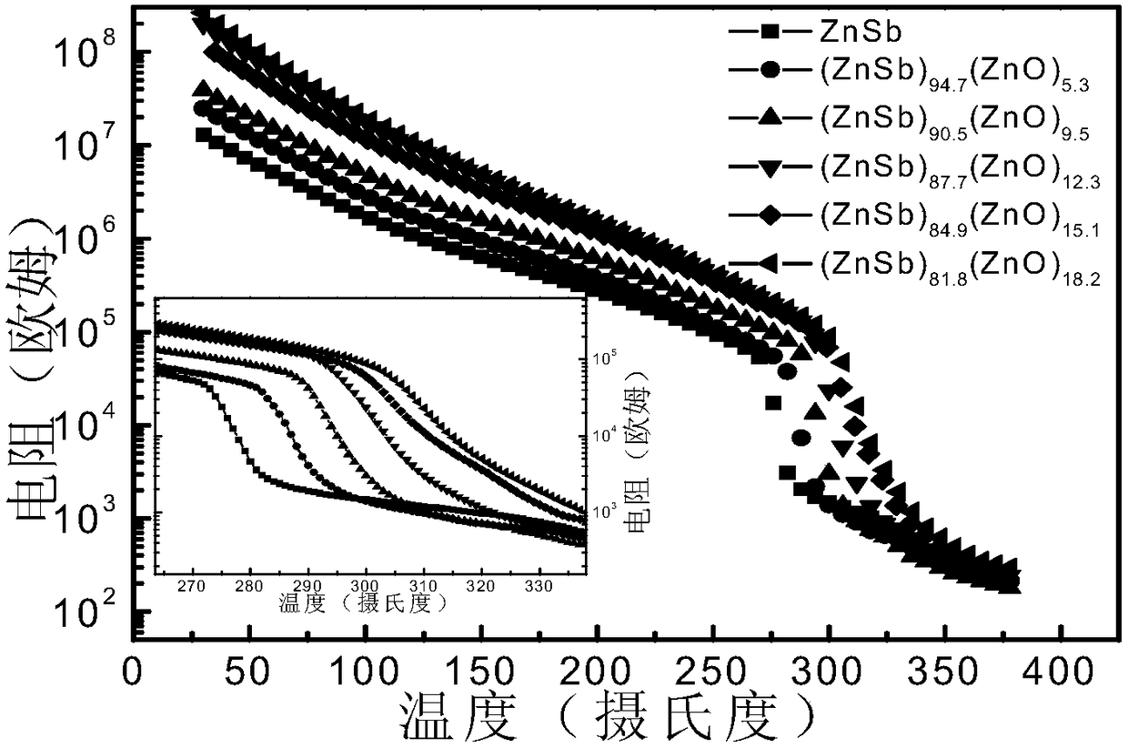
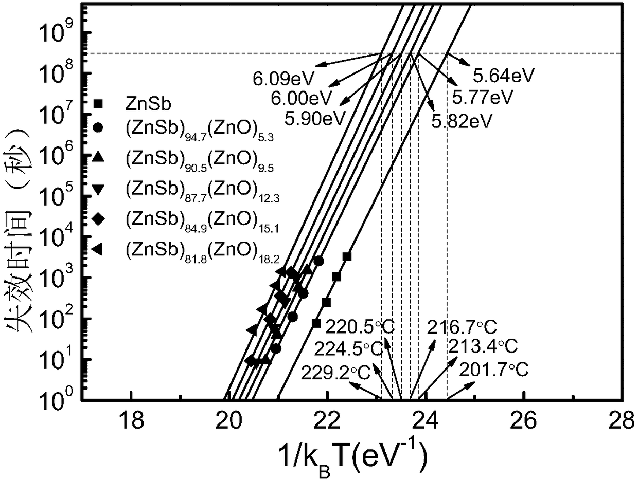
[0026] The prepared thin film material is tested for in-situ resistance, and the test results are as follows figure 1 with figure 2 Shown from figure 1 with figure 2 It can be seen that the performance indicators of the film prepared in this example are as follows: crystallization temperature T c It is 287℃, the highest temperature of ten-year retention capacity is 216.7℃, and the amorphous / crystalline resistance ratio is 2.20×10 5 .
Embodiment 3
[0028] The difference is that during the sputtering process, the sputtering power of the ZnO ceramic target is controlled to 12W, and the sputtering power of the ZnSb alloy target is 35W. The two targets are co-sputtered and coated at room temperature, and the sputtering thickness After 180 nm, the as-deposited nanocomposite (ZnSb) is obtained 100-x (ZnO) x Phase change storage film material. Where x=12.3, that is, the chemical structure is (ZnSb) 87.7 (ZnO) 12.3 .
[0029] The prepared thin film material is tested for in-situ resistance, and the test results are as follows figure 1 with figure 2 Shown from figure 1 with figure 2 It can be seen that the performance indicators of the film prepared in this example are as follows: crystallization temperature T c It is 294℃, the highest temperature of ten-year retention capacity is 220.5℃, and the amorphous / crystalline resistance ratio is 7.29×10 5 .
PUM
| Property | Measurement | Unit |
|---|---|---|
| crystallization temperature | aaaaa | aaaaa |
| crystallization temperature | aaaaa | aaaaa |
| temperature | aaaaa | aaaaa |
Abstract
Description
Claims
Application Information
 - R&D
- Intellectual Property
- Life Sciences
- Materials
- Tech Scout
- Unparalleled Data Quality
- Higher Quality Content
- 60% Fewer Hallucinations
Browse by: Latest US Patents, China's latest patents, Technical Efficacy Thesaurus, Application Domain, Technology Topic, Popular Technical Reports.
© 2025 PatSnap. All rights reserved.Legal|Privacy policy|Modern Slavery Act Transparency Statement|Sitemap|About US| Contact US: help@patsnap.com