Multi-channel microfluidic chip device for vacuum negative pressure injection, preparation method and application
A microfluidic chip and vacuum negative pressure technology, applied in chemical instruments and methods, laboratory containers, laboratory utensils, etc., can solve the complex manufacturing process, unsuitable for instant diagnosis applications, insufficient accurate quantitative sensing, etc. problem, to achieve the effect of less sample consumption, high-throughput accurate quantitative sensing, and accurate quantitative sensing
- Summary
- Abstract
- Description
- Claims
- Application Information
AI Technical Summary
Problems solved by technology
Method used
Image
Examples
Embodiment 1
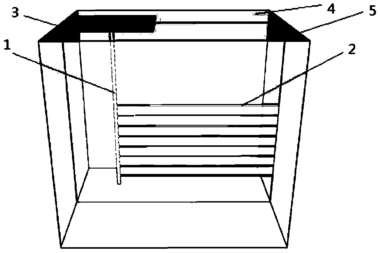
[0052] In this embodiment, the multi-channel microfluidic chip detection device for vacuum negative pressure sampling and blood filtration is composed of a microfluidic chip and a microporous filter membrane. Such as figure 1 As shown, the microfluidic chip is a polydimethylsiloxane (PDMS) microfluidic chip, which is formed by bonding a thin layer of PDMS engraved with a microchannel structure and a thin layer of PDMS without microchannels.
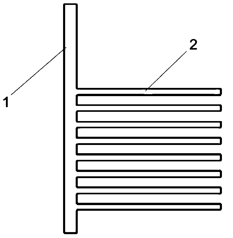
[0053] The microchannel structure in the PDMS thin layer is a main channel and eight parallel loading channels connected vertically. The structure of the entire microchannel is similar to the shape of a comb, such as figure 2 Shown.
[0054] In this embodiment, the eight sample loading channels are located on the same side of the main channel, and the channel width and the distance between the channels are set to be the same. The solution enters from the main channel port 1 and then disperses into eight tributaries into the sample loading chan...
Embodiment 2
[0058] The preparation method of the multi-channel microfluidic chip device with vacuum negative pressure sampling in the present invention includes the following steps:
[0059] (1) For the production of PDMS microfluidic chip, see Figure 4 , The specific production process can be divided into the following steps:
[0060] (1-1) Mask design and production: design the mask pattern of the microfluidic chip, and print the mask pattern on the film through a printer (resolution greater than 20000dpi) to obtain the film mask.
[0061] (1-2) Substrate cleaning and homogenization: After the substrate is strictly cleaned with acetone, Piranha solution and ultrapure water and dried at high temperature (150℃×1h), a proper amount of SU-8 photoresist is added to the center of the substrate. (About 1ml / inch 2 ), placed on the turntable of the glue homogenizer, and homogenized the glue using a program of 600rpm×18s, 2100rpm×60s (increasing the speed at a speed of 100rpm / min). The whole process o...
Embodiment 3
[0078] A multi-channel microfluidic chip detection device with vacuum negative pressure sampling and blood filtration. The microfluidic chip is formed by bonding a thin layer of polydimethylsiloxane (PDMS) engraved with microchannels and a thin layer of PDMS without microchannels. Make a cross cut on the two bonded PDMS to expose the main channel of the microchannel, apply a layer of glue at a certain distance around the exposed main channel opening, and glue a small piece of BTS film on the glue to make the main channel opening It is sealed, thus constituting the final chip device.
[0079] The microchannel structure is composed of one inlet channel and eight outlet channels connected, and its structural features are as follows: the solution inlet channel (hereinafter referred to as the main channel) is a straight channel connected to eight solution outlet channels (hereinafter referred to as the loading channel). The eight sample loading channels are arranged in parallel, with...
PUM
 Abstract
Description
Claims
Application Information


