Light emitting diode epitaxial wafer and manufacturing method thereof

A technology of light-emitting diodes and manufacturing methods, which is applied to electrical components, circuits, semiconductor devices, etc., can solve problems such as reducing LED luminous efficiency, and achieve the effects of reducing the number of electrons, improving luminous efficiency, and improving crystal quality

Active Publication Date: 2018-05-29
HC SEMITEK ZHEJIANG CO LTD
View PDF5 Cites 20 Cited by
  • Summary
  • Abstract
  • Description
  • Claims
  • Application Information

AI Technical Summary

Problems solved by technology

[0007] In order to solve the problem of reducing the luminous efficiency of LEDs in the prior art, an embodime

Method used


Image

  • Light emitting diode epitaxial wafer and manufacturing method thereof
  • Light emitting diode epitaxial wafer and manufacturing method thereof
  • Light emitting diode epitaxial wafer and manufacturing method thereof

Examples


Embodiment 1

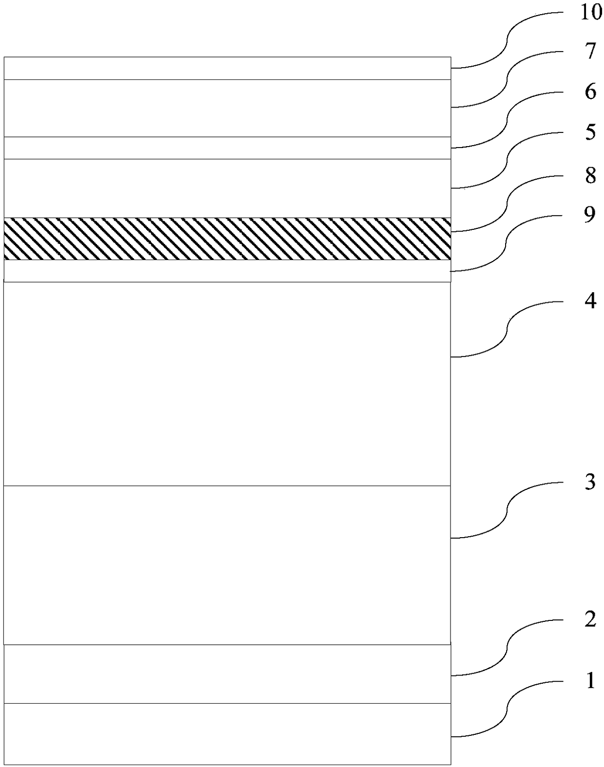
[0030] The embodiment of the present invention provides a light-emitting diode epitaxial wafer, figure 1 For a schematic structural diagram of the light-emitting diode epitaxial wafer provided in this embodiment, see figure 1 , the light-emitting diode epitaxial wafer includes a substrate 1 and a buffer layer 2, an undoped gallium nitride layer 3, an N-type gallium nitride layer 4, a multiple quantum well layer 5, a first electron blocking layer stacked on the substrate 1 in sequence layer 6 and p-type gallium nitride layer 7.

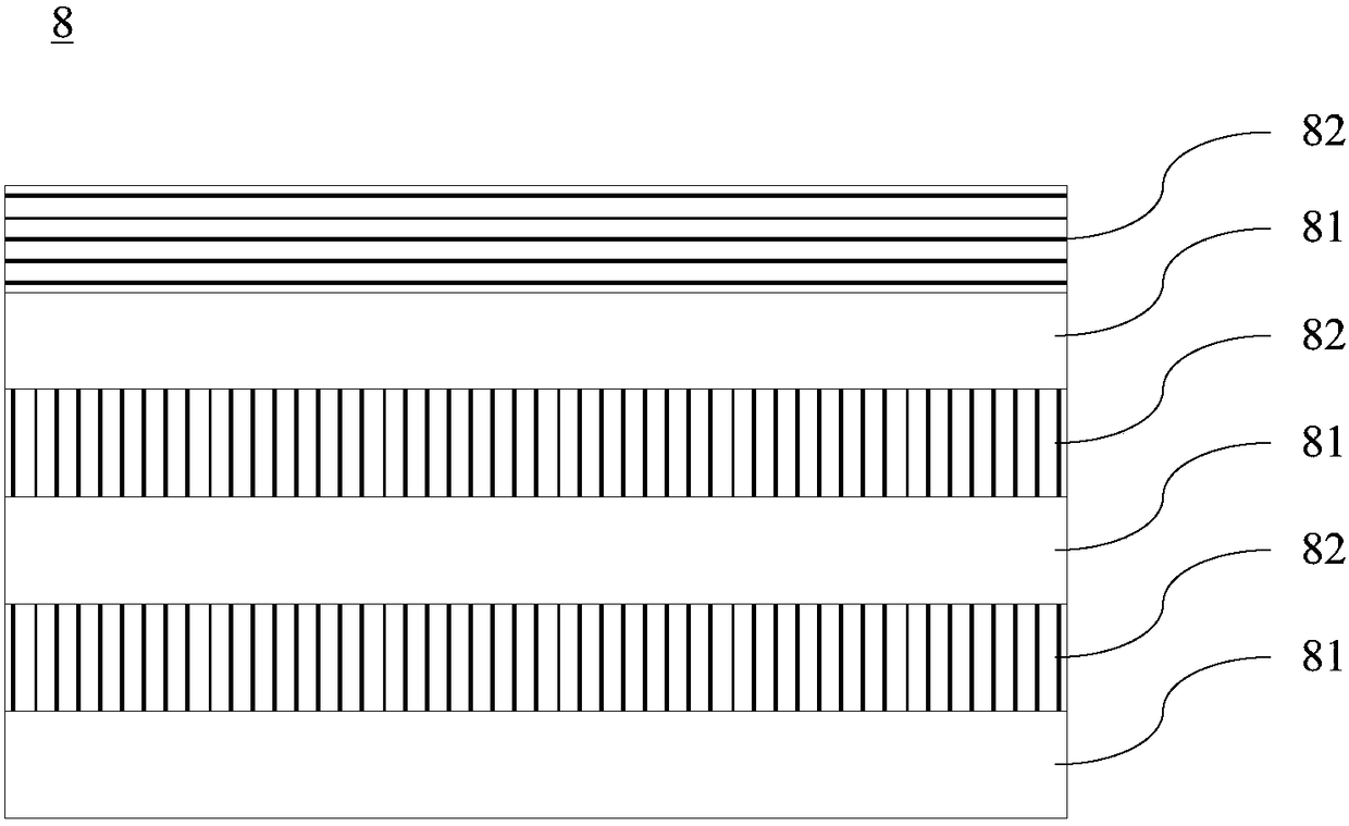
[0031] In this embodiment, the light-emitting diode epitaxial wafer further includes a second electron blocking layer 8 stacked between the N-type gallium nitride layer 4 and the multiple quantum well layer 5 . figure 2 For a schematic structural diagram of the second electron blocking layer provided in this embodiment, see figure 2 , the second electron blocking layer 8 includes a plurality of first sublayers 81 and a plurality of second sublayers...

Embodiment 2

[0071] An embodiment of the present invention provides a method for manufacturing a light-emitting diode epitaxial wafer, which is suitable for manufacturing the light-emitting diode epitaxial wafer provided in Embodiment 1.

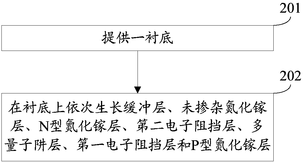
[0072] specifically, image 3 For the flow chart of the manufacturing method provided in this embodiment, see image 3 , the manufacturing method includes:

[0073] Step 201: Provide a substrate.

[0074] Step 202: sequentially growing a buffer layer, an undoped GaN layer, an N-type GaN layer, a second electron blocking layer, a multi-quantum well layer, a first electron blocking layer, and a P-type GaN layer on the substrate .

[0075] In this embodiment, the second electron blocking layer includes a plurality of first sublayers and a plurality of second sublayers, and the plurality of first sublayers and the plurality of second sublayers are alternately stacked. Each of the multiple first sublayers is an undoped indium gallium nitride layer, and th...

Embodiment 3

[0097] An embodiment of the present invention provides a method for manufacturing a light-emitting diode epitaxial wafer, and the manufacturing method provided in this embodiment is a specific realization of the manufacturing method provided in Embodiment 2. Figure 4 For the flow chart of the manufacturing method provided in this embodiment, see Figure 4 , the manufacturing method includes:

[0098] Step 301: Control the processing temperature to 600° C. and the sputtering pressure to 28 mTorr, and sputter an aluminum target in a nitrogen atmosphere to form an aluminum nitride layer in a buffer layer on the substrate.

[0099] Step 302: Control the growth temperature to 550° C., grow a gallium nitride layer with a thickness of 40 nm, and form a gallium nitride layer in a buffer layer on the aluminum nitride layer.

[0100] Step 303: Control the growth temperature to 1000° C., and grow a non-doped gallium nitride layer with a thickness of 1 μm on the buffer layer.

[0101] ...


PUM

PropertyMeasurementUnit
Thicknessaaaaaaaaaa
Thicknessaaaaaaaaaa
Thicknessaaaaaaaaaa

Abstract

The invention discloses a light emitting diode epitaxial wafer and a manufacturing method thereof, belonging to the technical field of semiconductors. The epitaxial wafer includes a substrate, a buffer layer, an undoped GaN layer, an N-type GaN layer, a second electron blocking layer, a multiple quantum well layer, a first electron blocking layer, and a P-type GaN layer. The electron blocking layer includes a plurality of first sub-layers and a plurality of second sub-layers that are alternately stacked. Each first sub-layer is an undoped indium gallium nitride layer, a second sub-layer of theplurality of second sub-layers closest to the multiple quantum well layer is a first aluminum gallium nitride layer, the first aluminum gallium nitride layer is an undoped aluminum gallium nitride layer, and each second sub-layer among the second sub-layers except the second sub-layer closest to the multiple quantum well layer is a second aluminum gallium nitride layer, the second aluminum gallium nitride layer is a P-type doped aluminum gallium nitride layer, and the doping concentration of a P-type dopant in each second aluminum gallium nitride layer is smaller than the doping concentrationof a P-type dopant in the GaN layer. The luminous efficiency can be improved.

Description

technical field [0001] The present invention relates to the technical field of semiconductors, in particular to a light emitting diode epitaxial wafer and a manufacturing method thereof. Background technique [0002] Light Emitting Diode (English: Light Emitting Diode, referred to as: LED) is a new generation of high-efficiency, environmentally friendly and green solid-state lighting sources, with low voltage, low power consumption, small size, light weight, long life, high reliability and other advantages. Rapid and widespread application. The core part of the LED is a chip, and the chip includes an epitaxial wafer and electrodes arranged on the epitaxial wafer. [0003] At present, the material of epitaxial wafer is mainly gallium nitride, which is a semiconductor material with a wide band gap (the band gap is about 3.4eV), which can generate blue light, and the generated blue light can get white light after passing through the yellow phosphor. Since the gallium-based LE...

Claims


Application Information

Patent Timeline
IPC IPC(8): H01L33/06H01L33/12H01L33/14H01L33/00
CPCH01L33/007H01L33/06H01L33/12H01L33/145
Inventor 兰叶顾小云黄龙杰王江波
Owner HC SEMITEK ZHEJIANG CO LTD
Why Eureka
Try Eureka