A two-dimensional material source follower with gas sensing function

A two-dimensional material and gas sensing technology, applied in the direction of material resistance, etc., can solve the problems of poor signal optimization, sensor signal influence, parasitic effects, etc., and achieve good energy band width and high carrier transfer rate , the effect of a good on-off ratio

Inactive Publication Date: 2020-04-28
HANGZHOU DIANZI UNIV
View PDF11 Cites 0 Cited by
  • Summary
  • Abstract
  • Description
  • Claims
  • Application Information

AI Technical Summary

Problems solved by technology

The sensor chip and IC need to be designed and processed separately. In the interconnection between the sensor and the IC, unnecessary parasitic effects, such as parasitic resistance and parasitic capacitance, are likely to occur, which will affect the sensing signal.
Moreover, the signal derived from the sensor is not well optimized, which increases the difficulty of peripheral circuits for sensor signal processing

Method used


Image

  • A two-dimensional material source follower with gas sensing function
  • A two-dimensional material source follower with gas sensing function
  • A two-dimensional material source follower with gas sensing function

Examples


Embodiment Construction

[0019] The present invention will be further described in detail below in conjunction with the accompanying drawings and specific embodiments.

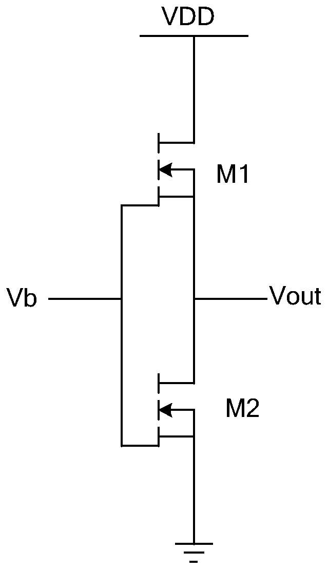
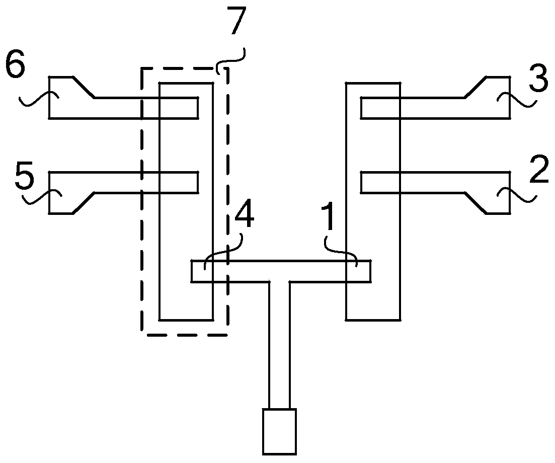
[0020] In order to realize the integrated system structure of sensor and circuit, the present invention adopts such as figure 1 The circuit structure of the source follower shown, figure 2 Shown is the layout structure diagram of the follower.

[0021] like figure 1 and 2 , the circuit of the source follower consists of two two-dimensional materials WS 2 fabricated transistors. The first NMOS transistor M1 is used as a gas sensor; the drain 1 of the first NMOS transistor M1 is connected to the power supply voltage VDD, and the gate 2 of the first NMOS transistor M1 is connected to the reference voltage Vb, so that the first NMOS transistor M1 works in the saturation region, and the first NMOS transistor M1 works in the saturation region. The source 3 of an NMOS transistor M1 is connected to the drain 4 of the second NMOS transis...


PUM

PropertyMeasurementUnit
thicknessaaaaaaaaaa
thicknessaaaaaaaaaa

Abstract

The invention relates to a two-dimensional material source follower with a gas sensing function. In interconnection of a sensor and an IC (Integrated Circuit), an existing product easily generates a parasitic effect which has influence to sensing signals. The two-dimensional material source follower provided by the invention comprises two transistors prepared from a two-dimensional material WS2, wherein M1 serves as a gas sensor; the drain electrode of the M1 is connected with power supply voltage, and the grid electrode of the M1 is connected with reference voltage so as to enable the M1 to work in a saturation region; the source electrode of the M1 is connected with the drain electrode of M2, and the grid electrode of the M2 is connected with reference voltage so as to enable the M2 of asecond NMOS (N-channel Metal Oxide Semiconductor) transistor M2 to work in the saturation region; the source electrode of the M2 is grounded, and the drain electrode of the M2 is connected with the output; and the M2 of the second NMOS transistor M2 is covered with an insulating material. The two-dimensional material source follower provided by the invention adopts the device structure that the transistors prepared from the two-dimensional material WS2 are adopted, and the sensor and a signal processing circuit are integrated on a wafer; and by designing the gas sensor and the signal processing circuit on the same wafer, the device structure is more compact, and the sensing performance is also greatly improved.

Description

technical field [0001] The invention belongs to the field of electronic devices and gas sensing, in particular to a two-dimensional material source follower with gas sensing function. Background technique [0002] In the traditional integrated circuit manufacturing process, silicon and doped silicon are usually used to manufacture transistors. The related technology is relatively mature, but the electrical performance of silicon material transistors is far inferior to that of two-dimensional materials (such as graphene or transition metal two Transistors made of sulfide (TMD)), currently, such transistors based on two-dimensional materials have not been able to realize complex integrated circuit systems due to the difficulty of obtaining materials and high manufacturing difficulties. [0003] For the existing gas sensors, the semiconductor materials used in most semiconductor gas sensors are mostly silicon and III-V and II-VI group element compounds, and their gas adsorption...

Claims


Application Information

Patent Timeline
Patent Type & Authority Patents(China)
IPC IPC(8): G01N27/12
CPCG01N27/12
Inventor 吴丽翔孙全胜王高峰
Owner HANGZHOU DIANZI UNIV
Why Eureka
Try Eureka