
Pulse laser film coating device

A pulsed laser, coating device technology, applied in sputtering coating, vacuum evaporation coating, ion implantation coating and other directions, can solve the problem of strip uniformity decline, non-uniformity, high evaporation energy, etc., to reduce the temperature drop Gradient, increasing the amount of YBCO, the effect of increasing the coating area

Active Publication Date: 2018-06-19
SHANGHAI SUPERCONDUCTOR TECH CO LTD
View PDF9 Cites 11 Cited by
  • Summary
  • Abstract
  • Description
  • Claims
  • Application Information

AI Technical Summary

Problems solved by technology

The reason is that pulsed laser deposition produces plasma instantaneously. Due to instantaneous evaporation, there is no preferential evaporation effect, and due to the axial confinement effect of instantaneous explosive expansion, the composition of the target material is basically the same as that of the film.
[0018] 2. Evaporation energy is high
At this time, the Yuhui shot again cannot be completely perpendicular to the target surface and the strip, so there will be some unevenness
[0035] The patent document US2005005846A1 proposes to use multiple targets and multiple laser beams from different lasers. Although it can speed up the deposition of coatings, it still has major limitations:
[0038] 3) The macroscopic pits on the surface of multiple targets are inconsistent, and the unevenness will be aggravated
If adjustment and optimization are not carried out, the sputtering efficiency of the pulse laser on the target will not reach the optimal range, and the energy of the pulse laser will be greatly wasted.
[0047] 3) For different targets, if the optical path is not optimized and adjusted according to its characteristics, the quality and efficiency of the sputtering coating process will be affected
[0052] 1) The coating process often needs to be carried out in a certain oxygen atmosphere, so the heating resistance wire has a short service life due to oxidation problems
[0053] 2) The heating and cooling speed of the resistance wire is relatively slow, and it is difficult to keep the temperature consistent
Although it can theoretically be used to heat the baseband, it also has great limitations:
[0055] 1) The high-frequency magnetic field will affect the surrounding equipment
[0056] 2) To make the heating uniform, it is necessary to make the magnetic field lines of each part of the workpiece cut more uniform, which is more difficult in the design
[0064] 1) If the tape running speed is fast and slow, there will be a large difference in the thickness of the film plated on the strip
[0065] 2) The heat capacity of the metal baseband is very small, and the stability and uniformity of the temperature field established by the radiation heating method in the deposition area will change due to the change of the airflow caused by the vibration of the baseband
[0073] 1) The focused pulsed laser beam also enters the coating cavity through a window, and the energy is lost again
[0074] 2) Due to the relative position of the chamber body wall and the target, it cannot be closer or further away, and the focus of the pulsed laser beam often makes some concessions
In order to meet this size, the purchase of the base material and the sale of the finished strip will inevitably cause a lot of waste due to the length deviation
[0078] 2) As the length of the production strip becomes longer, the volume of the equipment becomes larger, and the increase in the length of the production strip is not sustainable
[0079] 3) The strip must be at the same position in the deposition area. A slight movement of the strip in the lateral or longitudinal direction will cause a change in the thickness of the deposited film, which will lead to a decrease in the uniformity of the strip
[0097] 4. Utilization control of consumables

Method used


Image

  • Pulse laser film coating device
  • Pulse laser film coating device
  • Pulse laser film coating device

Examples


Embodiment Construction

[0188] The present invention will be described in detail below in conjunction with specific embodiments. The following examples will help those skilled in the art to further understand the present invention, but do not limit the present invention in any form. It should be noted that those skilled in the art can make several changes and improvements without departing from the concept of the present invention. These all belong to the protection scope of the present invention.

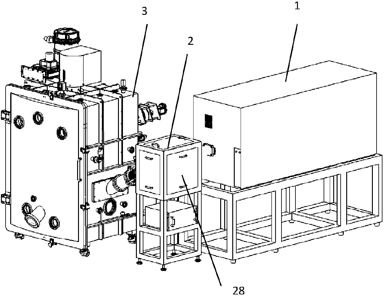
[0189] A pulse laser coating device according to the present invention is used to coat superconducting layers on multi-lane reciprocatingly wound base tape 336 , including a laser 1 , an optical system 2 , a coating chamber 3 , and a control and monitoring system 4 .

[0190] The laser 1 is mainly composed of one or more lasers, which can generate a pulsed laser beam 21;

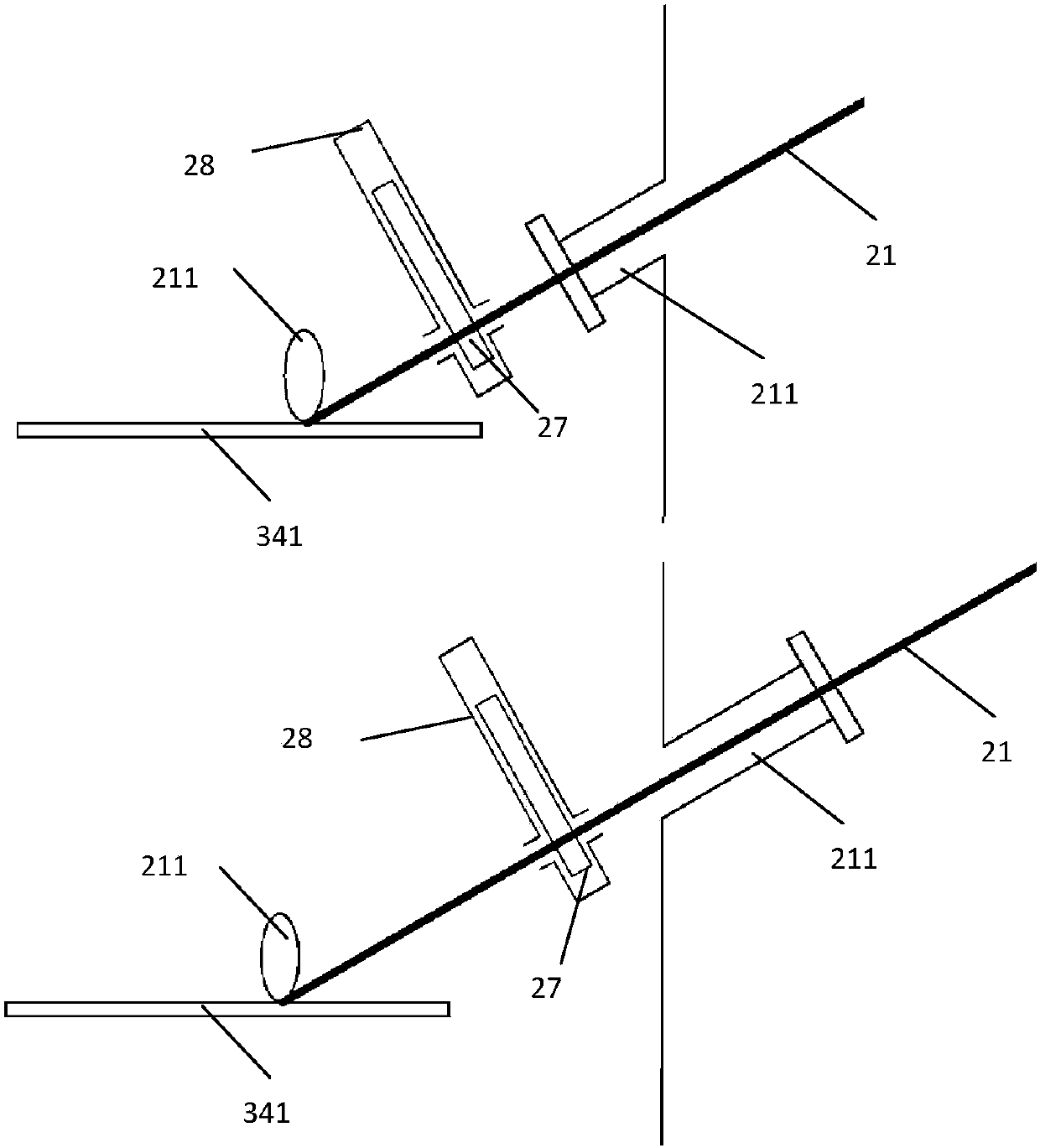
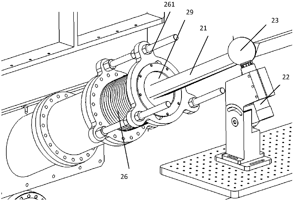
[0191] The optical path system 2 includes at least one or more groups of lenses 24, and the pulsed laser beam 21 generated by the la...


PUM

PropertyMeasurementUnit
thicknessaaaaaaaaaa
thicknessaaaaaaaaaa

Abstract

The invention provides a pulse laser film coating device. The pulse laser film coating device comprises a laser (1), an optical path system (2), and a film coating cavity body (3), wherein the laser (1) produces a pulse laser beam (21); and the optical path system (2) is used for leading the pulse laser beam (21) into the film coating cavity body (3), so that plumes (211) are formed in the surfaceof a target material (341) and a material of the target material (341) is sputtered onto a base band (226) to form a superconducting layer. According to the pulse laser film coating device disclosedby the invention, the quality and the quantity of pulse laser coating films can be improved, and the use of equipment also can be improved.

Description

technical field [0001] The present invention relates to the technical field of superconducting materials, more specifically, to a pulsed laser coating device, in particular to a manufacturing device for a superconducting layer of a second-generation high-temperature superconducting strip. Background technique [0002] Since the first discovery of superconductivity in the laboratory by Professor Camerin Onners of Leiden University in the Netherlands in 1911, superconducting materials and their applications have been one of the most active frontier research fields in contemporary science and technology. In the past ten years, the research on superconducting power devices based on superconductivity has developed rapidly. In superconducting energy storage, superconducting motors, superconducting cables, superconducting current limiters, superconducting transformers, superconducting magnetic levitation, Remarkable achievements have been made in fields such as nuclear magnetic res...

Claims


Application Information

Patent Timeline
Patent Type & Authority Applications(China)
IPC IPC(8): C23C14/34C23C14/08C23C14/56
CPCC23C14/08C23C14/34C23C14/54C23C14/562
Inventor 朱佳敏陈思侃赵跃张智巍吴祥姚林朋
Owner SHANGHAI SUPERCONDUCTOR TECH CO LTD
Learn More