Optical fiber surface enhanced raman probe based on surface plasmon effect and manufacturing method thereof

A surface plasmon, surface-enhanced Raman technology, applied in Raman scattering, material excitation analysis, material analysis by optical means, etc., can solve problems such as background interference, and achieve the effect of simple structure

Pending Publication Date: 2018-06-19
NANJING UNIV OF INFORMATION SCI & TECH
View PDF0 Cites 9 Cited by
  • Summary
  • Abstract
  • Description
  • Claims
  • Application Information

AI Technical Summary

Problems solved by technology

[0007] The purpose of the present invention is to overcome the deficiencies in the prior art, provide a fiber surface-enhanced Raman probe based on the surface plasmon effect and its manufacturing method, and solve the technical problem of background interference in the prior art, In addition, this solution simplifies the detection. The position of the microscopic area that is not suitable for the microscope system can be directly sampled by the fiber optic probe for detection, while taking into account the characteristics of portability, trace detection and low noise.

Method used


Image

  • Optical fiber surface enhanced raman probe based on surface plasmon effect and manufacturing method thereof
  • Optical fiber surface enhanced raman probe based on surface plasmon effect and manufacturing method thereof
  • Optical fiber surface enhanced raman probe based on surface plasmon effect and manufacturing method thereof

Examples


Embodiment Construction

[0025] The present invention will be further described below in conjunction with the accompanying drawings. Following examples are only used to more clearly illustrate technical scheme of the present invention, and can not limit protection scope of the present invention with this.

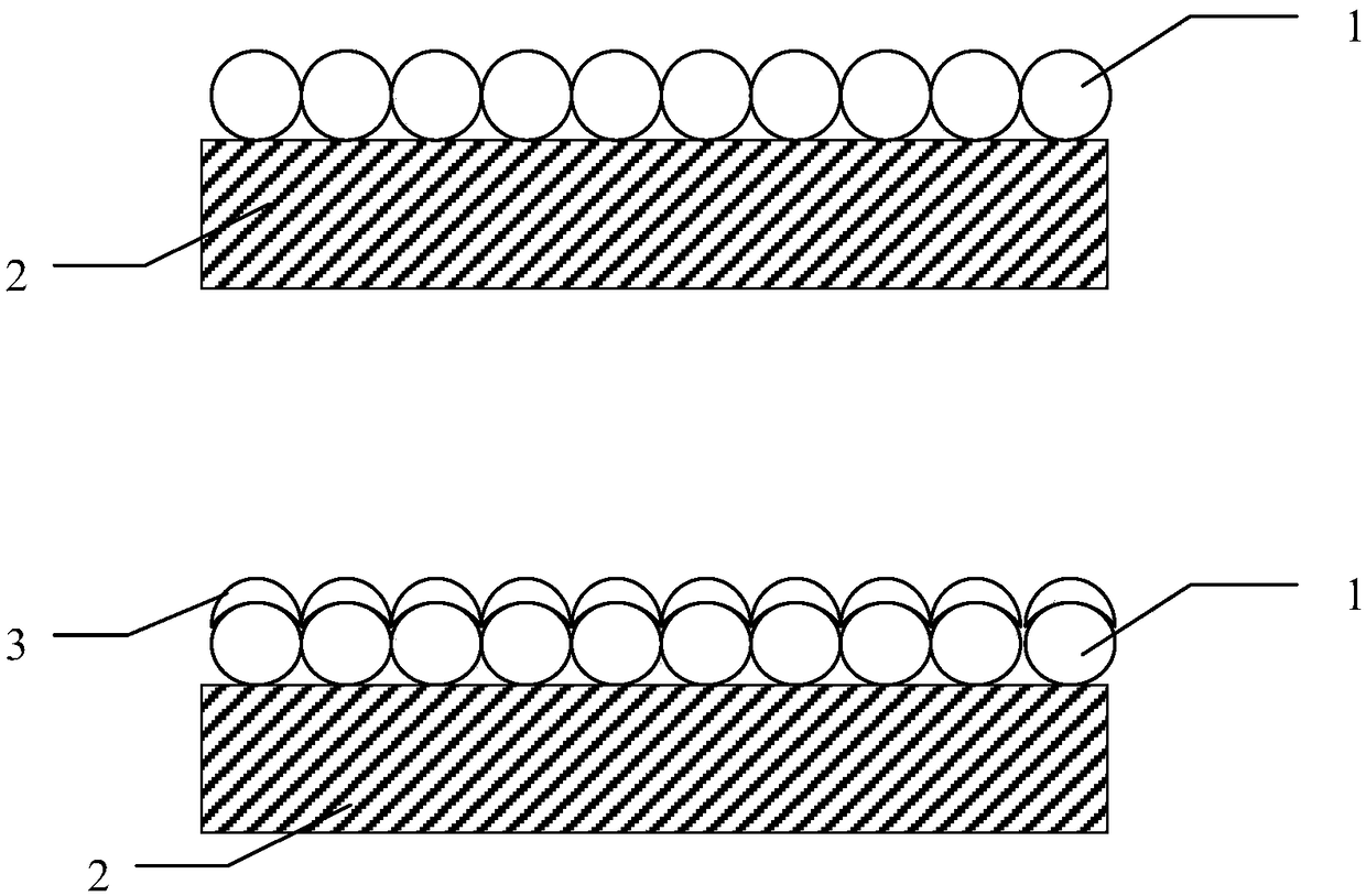
[0026] Such as figure 1 As shown, it is a schematic diagram of the SERS substrate, including a quartz substrate 2, on which a polystyrene (PS) nanoscale microsphere array is arranged, and the top of the PS microsphere array 1 is also covered with a metallic silver film 3 , forming a hemispherical metallic silver array, and the microsphere array may have certain defects.

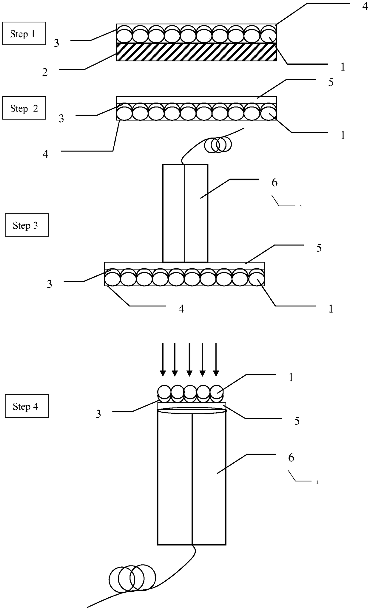
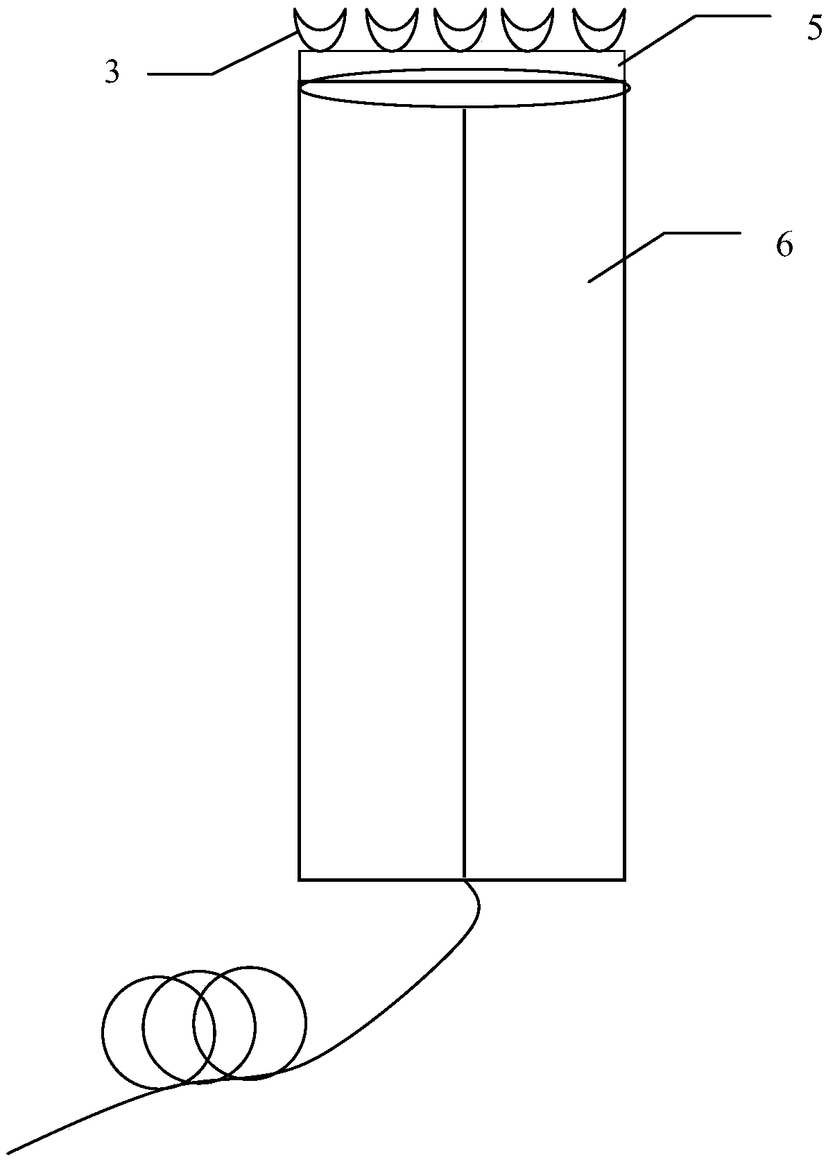
[0027] The flow chart of the present invention is as figure 2 As shown, the PMMA photoresist 4 is evenly filled between the PS microsphere arrays 1, and the Noa glue 5 is coated on the surface of the PMMA photoresist 4, after the film of the quartz substrate 2 is removed and transferred to the optical fiber This structure can ...


PUM


Abstract

The invention discloses an optical fiber surface enhanced raman probe based on surface plasmon effect and a manufacturing method thereof. A layer of periodic metal structure is adhered to a grinded optical fiber end surface. The manufacturing method comprises the following steps: spin-coating a PS microsphere array on a base plate, partially etching and a coating a metal film on the top of the PSmicrosphere to form a hemispherical metal structure, spin-coating polymer on the surface of the hemispherical metal surface and curing, and removing substrate; curing the obtained film with the optical fiber end surface with glue, completely removing the PS microsphere after curing, performing RIE etching to regulate the geometric dimension of the metal structure for enabling resonant wavelength of the metal structure to be consistent with excited laser wavelength, and only leaving a metal hemispherical array on the top of the optical fiber. A to-be-measured sample is adsorbed on the surface of the metal hemispherical array, a light source couples and enters from one end of the optical fiber, and the metal structure is irradiated from the inner part of the optical fiber, so that a measurable raman signal is generated by laser under action of the metal structure, and the laser is output and analyzed by a spectrograph after being collected by the optical fiber. The optical fiber surfaceenhanced raman probe is simple in structure and is suitable for processing production.

Description

technical field [0001] The invention relates to an optical fiber surface-enhanced Raman probe based on the surface plasmon effect and a manufacturing method thereof, belonging to the technical field of photochemical sensors. Background technique [0002] In traditional Raman spectroscopic analysis, for samples such as liquids, films, and powders, satisfactory spectra can be obtained without special sample processing, but for some inhomogeneous samples or samples that are not convenient for direct sampling, it is necessary to Fiber Raman Probe. The Raman scattering signal is collected by the optical fiber Raman probe, and the signal is transmitted to the detector through the optical fiber to obtain the Raman spectrum. Trace detection, repeatable detection. Local tissue detection. The application of optical fiber in Raman spectroscopy greatly simplifies the optical system of traditional spectroscopy methods and improves the measurement range of spectroscopy instruments. It ...

Claims


Application Information

Patent Timeline
IPC IPC(8): G01N21/65
CPCG01N21/658
Inventor 倪海彬葛璐潘超周盈常建华王婷婷葛益娴
Owner NANJING UNIV OF INFORMATION SCI & TECH
Why Eureka
Try Eureka