
Graphene field effect transistor quantum dot photoelectric detector and manufacturing method

A technology of field-effect transistors and photodetectors, applied in the field of photoelectric detection, can solve problems such as restricted applications and poor mobility of quantum dots, and achieve the goal of improving the non-dense film, good optical properties and chemical stability, and increasing mobility. Effect

Active Publication Date: 2018-06-22
NANJING UNIV OF POSTS & TELECOMM +1
View PDF6 Cites 4 Cited by
  • Summary
  • Abstract
  • Description
  • Claims
  • Application Information

AI Technical Summary

Problems solved by technology

However, as a semiconductor material, quantum dots have extremely poor mobility, which has restricted their application in photodetectors.

Method used


Image

  • Graphene field effect transistor quantum dot photoelectric detector and manufacturing method
  • Graphene field effect transistor quantum dot photoelectric detector and manufacturing method
  • Graphene field effect transistor quantum dot photoelectric detector and manufacturing method

Examples


Embodiment 1

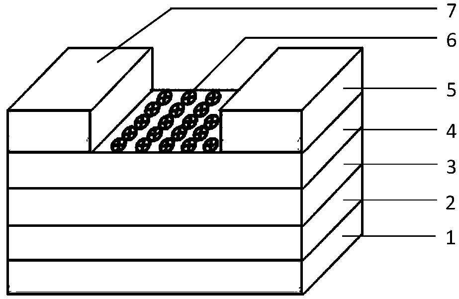
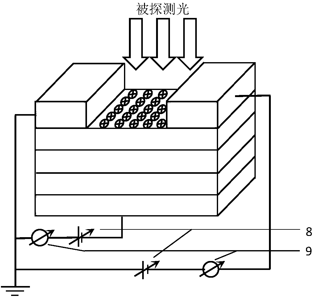
[0028] like figure 1 Shown, a kind of graphene field effect transistor quantum dot photodetector, this photodetector is a multilayer film structure, comprises Si substrate layer 1, first insulation layer 2, second insulation layer 3, graphene channel layer 4 , quantum dot photosensitive medium layer 6 and source 7 and drain 5; the Si substrate layer 1, first insulating layer 2, second insulating layer 3, graphene channel layer 4, quantum dot photosensitive medium layer 6 from below stacked sequentially at the top; the source electrode 5 and the drain electrode 8 are respectively located on the left and right sides of the quantum dot photosensitive medium layer 6 . like figure 2 As shown, when the performance of the photodetector is tested, the source 7, the drain 5 and the Si substrate layer 1 as the gate are electrically connected through an adjustable DC voltage source 8, a micro ammeter 9 and several unmarked connecting power lines.

[0029] The material of the Si substr...


PUM


Abstract

The invention relates to the photoelectric detection field and especially relates to a graphene field effect transistor quantum dot photoelectric detector and a manufacturing method. The photoelectricdetector is a multilayer film structure and comprises a Si substrate layer, a first insulating layer, a second insulating layer, a graphene channel layer, a quantum dot photosensitive dielectric layer, a source electrode and a drain electrode. On a substrate, thermal oxidation is performed so as to grow first insulating layer silicon oxide, a magnetron sputtering method is used to grow second insulating layer aluminum nitride which is taken as a double-insulating layer, and an enhanced chemical vapor deposition method is used to grow a graphene layer on the double-insulating layer. The two ends of the graphene layer are provided with the source electrode and the drain electrode. One quantum dot photosensitive dielectric layer is coated between the source electrode and the drain electrode.In the invention, through designing a reasonable device structure, under an illumination condition, a quantum dot and graphene can generate effective charge transfer so that light with a specific frequency is converted into a light current, and finally, incident light can be effectively detected.

Description

technical field [0001] The invention relates to the field of photoelectric detection, in particular to a graphene field effect transistor quantum dot photodetector and a preparation method thereof. Background technique [0002] A photodetector is an instrument that converts optical signals into electrical signals. Its basic principle is to use light radiation to cause changes in the conductivity of the irradiated material, thereby causing changes in electrical signals. Photoelectric detectors are widely used in many fields of military and national economy. They are mainly used for ray measurement and detection, industrial automatic control, photometry, etc. in the visible or near-infrared band; they are mainly used in missile guidance, infrared thermal imaging, infrared remote sensing etc. With the development of laser and infrared technology, as well as the improvement of material performance and the continuous improvement of manufacturing process, photodetectors are devel...

Claims


Application Information

Patent Timeline
Patent Type & Authority Applications(China)
IPC IPC(8): H01L31/113H01L31/028H01L31/0216H01L31/18
CPCH01L31/02161H01L31/028H01L31/113H01L31/1804Y02P70/50
Inventor 郑加金王雅茹余柯涵韦玮胡二涛
Owner NANJING UNIV OF POSTS & TELECOMM
Learn More