Copper thin film preparation method
A technology of copper thin film and copper compound, which is applied in the direction of liquid chemical plating, metal material coating process, coating, etc., can solve the problems of complex process, large coating stress, difficult film separation, etc., and achieve uniform physical properties, thickness Uniform and controllable, easy-to-operate effect
- Summary
- Abstract
- Description
- Claims
- Application Information
AI Technical Summary
Problems solved by technology
Method used
Image

Examples
preparation example Construction
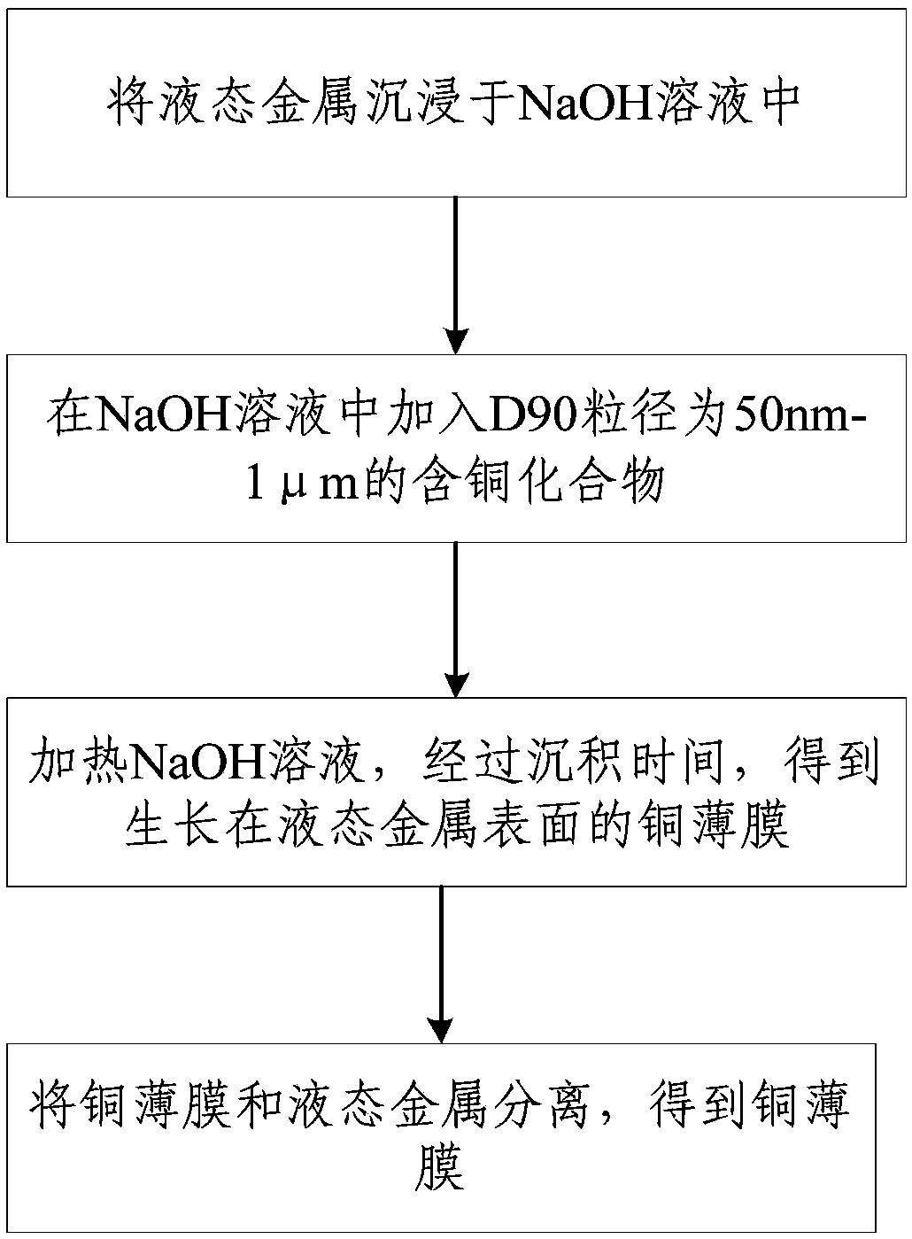
[0025] figure 1 Is a schematic diagram of a method for preparing a copper film according to a preferred embodiment of the present invention, such as figure 1 As shown, the present invention provides a method for preparing a copper film, which includes: using liquid metal as a deposition template, and a NaOH solution as a deposition liquid medium, adding a copper-containing compound to the NaOH solution to prepare a copper film.
[0026] Specifically, in this embodiment, NaOH solution is used as the deposition liquid medium, liquid metal is immersed in the NaOH solution as the deposition template, and the copper-containing compound is added to the NaOH solution to cause the copper-containing compound to undergo a reduction reaction in the NaOH solution, so that the The prepared copper film is formed on the metal surface.
[0027] figure 2 Is a flow chart of a method for preparing a copper film according to a preferred embodiment of the present invention, such as figure 2 As shown, ...
Embodiment 1
[0043] S1. 5 parts of liquid metal with 75.5wt% Ga and 24.5wt% In are added to 10 parts of NaOH solution with a concentration of 1mol / L to precipitate the liquid metal in the NaOH solution;
[0044] S2. Add 1 part of CuO powder with D90 particle size of 50nm and purity of 99.99% to the NaOH solution;
[0045] S3. Heat the NaOH solution to 50°C in a water bath, and the CuO powder undergoes a reduction reaction. After a deposition time of 12 hours, a copper film grown on the surface of the liquid metal is obtained;
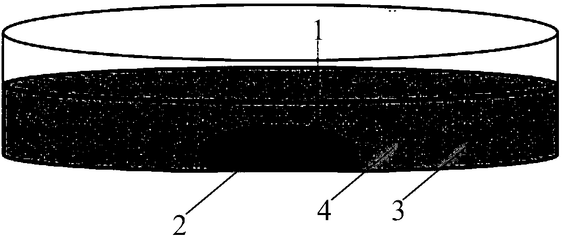
[0046] S4. Extract the liquid metal on which the copper film is grown on the surface, separate the liquid metal and the copper film to obtain a copper film, and test its phase.
[0047] image 3 Is the SEM cross-sectional view of the copper film prepared according to the embodiment of the present invention, such as image 3 As shown, it can be seen that the copper film prepared in Example 1 is composed of nano-copper and has a thickness of about 300 nm.
Embodiment 2
[0049] S1. Add 10 parts of liquid metal with a composition of 68.5wt% Ga, 20.5wt% In and 10.5wt% Sn to 10 parts of NaOH solution with a concentration of 0.5mol / L to precipitate the liquid metal in the NaOH solution;
[0050] S2. Add 0.01 parts of CuO powder with a D90 particle size of 50nm and a purity of 99.99% and 0.01 parts of CuCl with a purity of 99.99% into the NaOH solution 2 Composition of copper-containing compounds;
[0051] S3. Heat the NaOH solution to 30°C in a water bath, and the copper-containing compound undergoes a reduction reaction. After a deposition time of 24 hours, a copper film grown on the surface of the liquid metal is obtained;
[0052] S4. Extract the liquid metal on which the copper thin film is grown on the surface, separate the liquid metal and the copper thin film to obtain a copper thin film, and test its microscopic morphology.
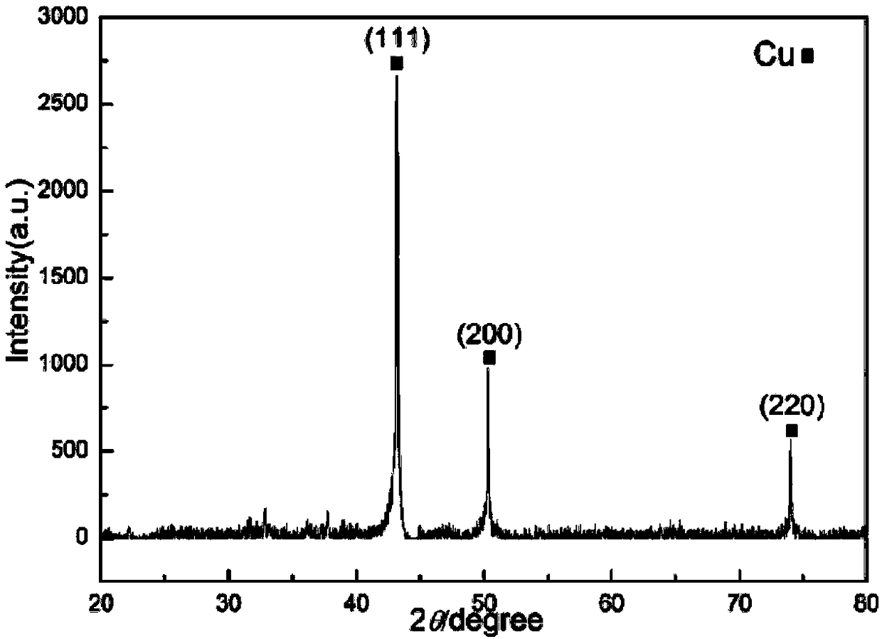
[0053] Figure 4 Is the XRD pattern of the copper thin film prepared according to the embodiment of the present invention, s...
PUM
| Property | Measurement | Unit |
|---|---|---|
| Thickness | aaaaa | aaaaa |
| Particle size | aaaaa | aaaaa |
Abstract
Description
Claims
Application Information
 - Generate Ideas
- Intellectual Property
- Life Sciences
- Materials
- Tech Scout
- Unparalleled Data Quality
- Higher Quality Content
- 60% Fewer Hallucinations
Browse by: Latest US Patents, China's latest patents, Technical Efficacy Thesaurus, Application Domain, Technology Topic, Popular Technical Reports.
© 2025 PatSnap. All rights reserved.Legal|Privacy policy|Modern Slavery Act Transparency Statement|Sitemap|About US| Contact US: help@patsnap.com