Local electromagnetic field enhancement device for Raman spectrum characterization as well as preparation method, application and utilization method thereof
A technology of Raman spectroscopy and electromagnetic field, applied in the field of detection, can solve the problems that it is difficult to obtain the difference of single-molecule configuration and conformation, and it is difficult to obtain Raman scattering signals on the single-molecule scale, so as to overcome the difference of configuration and conformation, Effect of enhancing Raman scattering signal and preventing oxidation of silver layer
- Summary
- Abstract
- Description
- Claims
- Application Information
AI Technical Summary
Problems solved by technology
Method used
Image
Examples
Embodiment 1
[0033] Fabrication of Localized Electromagnetic Field Enhanced Devices for Raman Spectroscopy Characterization
[0034] (1) Preparation of composite metal nanohole array substrate
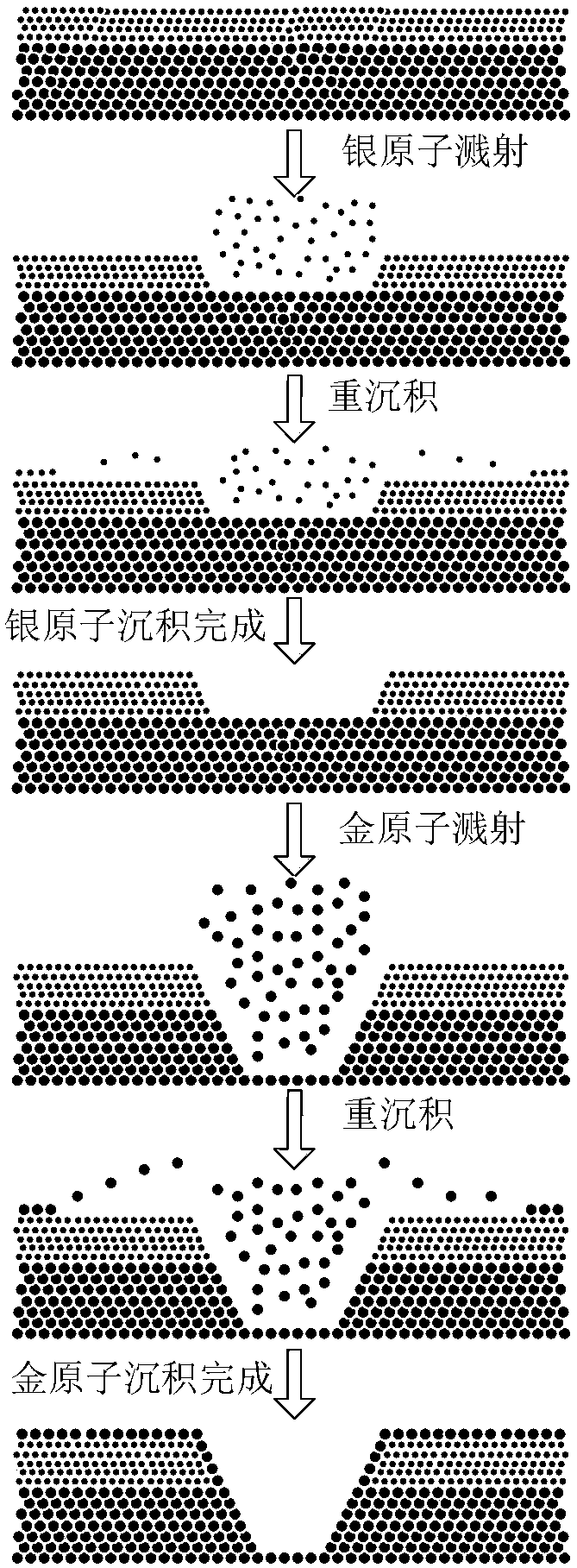
[0035] see figure 1 The flow chart of the preparation process of the composite metal nanohole array substrate. After the glass sheet 1 is cleaned by a plasma cleaning machine, a 2nm thick chromium layer 2 and a 100nm thick gold layer 3 are sequentially deposited from bottom to top using vacuum evaporation technology and a silver layer 4 with a thickness of 20nm, and then use the focused ion beam etching technique (etching principle see figure 2 ), using a gallium source, using a 15μm aperture, when the beam current is less than 5pA, the focused ion beam dose is 0.1nC / μm 2 Under the above conditions, the silver layer 4 is first etched, and the silver atoms sputtered during the etching process are re-deposited on the unetched place of the silver layer 4. After the silver layer 4 is etched through,...
Embodiment 2
[0039] Fabrication of Localized Electromagnetic Field Enhanced Devices for Raman Spectroscopy Characterization
[0040] (1) Preparation of composite metal nanohole array substrate
[0041] see figure 1 Process flow chart for the preparation of the composite metal nanohole array substrate. After cleaning the glass sheet 1 with a plasma cleaner, a 3nm-thick chromium layer 2 and a 50nm-thick gold layer 3 are sequentially deposited from bottom to top using vacuum evaporation technology. and a silver layer 4 with a thickness of 35nm, and then use the focused ion beam etching technique (etching principle see figure 2 ), using a gallium source, using a 15μm aperture, when the beam current is less than 5pA, the focused ion beam dose is 0.05nC / μm 2 Under the above conditions, the silver layer 4 is first etched, and the silver atoms sputtered during the etching process are re-deposited on the unetched place of the silver layer 4. After the silver layer 4 is etched through, the gold l...
Embodiment 3
[0045] Fabrication of Localized Electromagnetic Field Enhanced Devices for Raman Spectroscopy Characterization
[0046] (1) Preparation of composite metal nanohole array substrate
[0047] see figure 1 The flow chart of the preparation process of the composite metal nanohole array substrate. After the glass sheet 1 is cleaned by a plasma cleaning machine, a 2nm thick chromium layer 2 and a 75nm thick gold layer 3 are sequentially deposited from bottom to top using vacuum evaporation technology. and a silver layer 4 with a thickness of 50nm, and then use focused ion beam etching (etching principle see figure 2 ), using gallium source, 15μm aperture, when the beam current is less than 5pA, the focused ion beam dose is 0.02nC / μm 2 Under the above conditions, the silver layer 4 is first etched, and the silver atoms sputtered during the etching process are re-deposited on the unetched place of the silver layer 4. After the silver layer 4 is etched through, the gold layer 3 is et...
PUM
| Property | Measurement | Unit |
|---|---|---|
| thickness | aaaaa | aaaaa |
| thickness | aaaaa | aaaaa |
| thickness | aaaaa | aaaaa |
Abstract
Description
Claims
Application Information


