A method for preparing a magnetic tunnel junction array

A magnetic tunnel junction and array technology, which is applied in the manufacture/processing of magnetic field-controlled resistors and electromagnetic devices, can solve the serious loss of mask layer and magnetic tunnel junction material, reduce the magnetic and electrical performance of magnetic tunnel junction, Unfavorable problems such as magnetic memory yield, to improve magnetic/electrical performance and yield, increase anisotropic etching performance, and be conducive to miniaturization

Active Publication Date: 2022-02-25
SHANGHAI CIYU INFORMATION TECH CO LTD
View PDF5 Cites 0 Cited by
  • Summary
  • Abstract
  • Description
  • Claims
  • Application Information

AI Technical Summary

Problems solved by technology

[0006] However, in the existing reactive ion etching (RIE) process, the selected chemically active gas often has a low etching selectivity ratio for the mask layer and the magnetic tunnel junction material, resulting in the mask layer and the magnetic tunnel junction material being damaged during the etching process. The material loss is serious. At the same time, the etching loss material is deposited on the side wall of the tunnel junction to form a damaged layer / deposited layer, which reduces the magnetic and electrical properties of the magnetic tunnel junction. The short circuit of the memory layer is not conducive to the improvement of the yield rate of the magnetic memory

Method used


Image

  • A method for preparing a magnetic tunnel junction array
  • A method for preparing a magnetic tunnel junction array
  • A method for preparing a magnetic tunnel junction array

Examples


Embodiment Construction

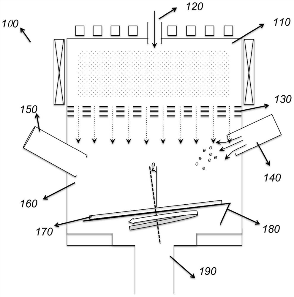
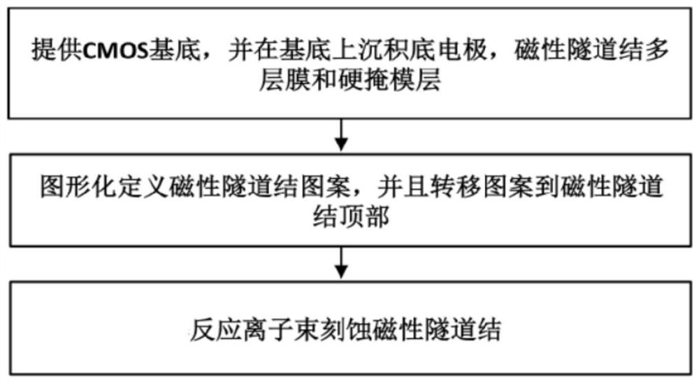
[0036] This embodiment provides a method for preparing a magnetic tunnel junction array by reactive ion beam etching, by using gases with carbonyl or hydroxyl functional groups, such as HCOOH, CH 3 OH, CH 3 COOH, C 2 h 5 OH, CO / NH 3 , as an ion source to etch the magnetic tunnel junction, and at the same time, perform small-angle ion beam trimming on the magnetic tunnel junction during and / or after etching. Its specific implementation steps are as follows figure 2 Shown:

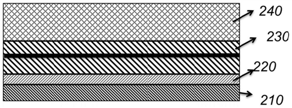
[0037] Step 1: Provide a CMOS substrate 210, and deposit a bottom electrode 220, a magnetic tunnel junction multilayer film 230 and a mask layer 230 on the substrate, such as image 3 shown;

[0038] Wherein, the bottom electrode 220 includes a seed layer and a conductive layer, the seed layer is Ta, TaN, W, WN, Ti or TiN, and the thickness of the seed layer is 0-5nm. In this embodiment, metal Ta is used to make a 3nm seed layer; The conductive layer is Cu, CuN, Mo, W or Ru, and the thickness of the ...


PUM

PropertyMeasurementUnit
thicknessaaaaaaaaaa
thicknessaaaaaaaaaa
thicknessaaaaaaaaaa

Abstract

The invention discloses a method for preparing a magnetic tunnel junction array, which relates to the technical field of magnetic random access memory manufacturing. The magnetic tunnel junction is etched by using a gas with carbonyl or hydroxyl functional groups as an ion source. The layer and the magnetic tunnel junction material have a relatively high selectivity ratio, which reduces the loss of the mask during the etching process, and the redeposition of the mask material and the redeposition of the magnetic tunnel junction material due to physical sputtering are beneficial. Preventing the formation of conductive channels in the memory layer and the reference layer has a significant effect on improving the magnetic / electrical performance and yield of the magnetic random access memory. At the same time, the ion beam has good directional properties, increases the anisotropic etching performance, and is beneficial to the miniaturization of magnetic random access memory devices.

Description

technical field [0001] The present invention relates to the field of magnetic random access memory (MRAM, Magnetic Radom Access Memory) manufacturing technology, in particular to a method for preparing a magnetic tunnel junction array by reactive ion beam etching (RIBE, Reactive Ion Beam Etching). Background technique [0002] In recent years, Magnetic Random Access Memory (MRAM, Magnetic Radom Access Memory) using Magnetic Tunnel Junction (MTJ, Magnetic Tunnel Junction) is considered to be the future solid-state non-volatile memory, which has high-speed reading and writing, large capacity and low energy consumption. consumption characteristics. Ferromagnetic MTJ is usually a sandwich structure, which has a magnetic memory layer, which can change the magnetization direction to record different data; an insulating tunnel barrier layer in the middle; a magnetic reference layer, located on the other side of the tunnel barrier layer, which The direction of magnetization remains...

Claims


Application Information

Patent Timeline
Patent Type & Authority Patents(China)
IPC IPC(8): H01L43/08H01L43/12
CPCH10N50/01H10N50/10
Inventor 张云森
Owner SHANGHAI CIYU INFORMATION TECH CO LTD
Why Eureka
Try Eureka