Check patentability & draft patents in minutes with Patsnap Eureka AI!

A method of making magnetic random access memory

A random access memory and storage device technology, applied in the field of manufacturing magnetic random access memory, manufacturing magnetic tunnel junction structural units and related logic units, can solve the problem of rapid diffusion of magnetic tunnel junction contamination copper, increase process complexity and production costs, and affect devices Issues such as magnetic and electrical properties

Active Publication Date: 2021-04-20
SHANGHAI CIYU INFORMATION TECH CO LTD
View PDF1 Cites 0 Cited by
  • Summary
  • Abstract
  • Description
  • Claims
  • Application Information

AI Technical Summary

Problems solved by technology

When etching the magnetic tunnel junction and its bottom electrode, due to over-etching, copper will be exposed to the plasma, which will cause copper to pollute the magnetic tunnel junction and copper in low dielectric constant (low-k ) rapid diffusion in the dielectric, thereby affecting the magnetic and electrical properties of the device
[0006] In order to realize the connection between the top electrode of the MTJ unit and the CMOS circuit, a through hole (Via) is usually made on the top of the MTJ unit for connection, which undoubtedly increases the complexity of the process and the production cost.

Method used


Image

  • A method of making magnetic random access memory
  • A method of making magnetic random access memory
  • A method of making magnetic random access memory

Examples


Embodiment Construction

[0045] In order to make the above objects, features and advantages of the present invention more comprehensible, specific implementations of the present invention will be described in detail below in conjunction with the accompanying drawings. It should be noted that all the drawings of the present invention are in simplified form and use inaccurate scales, and are only used to facilitate and clearly assist the purpose of illustrating the embodiments of the present invention.

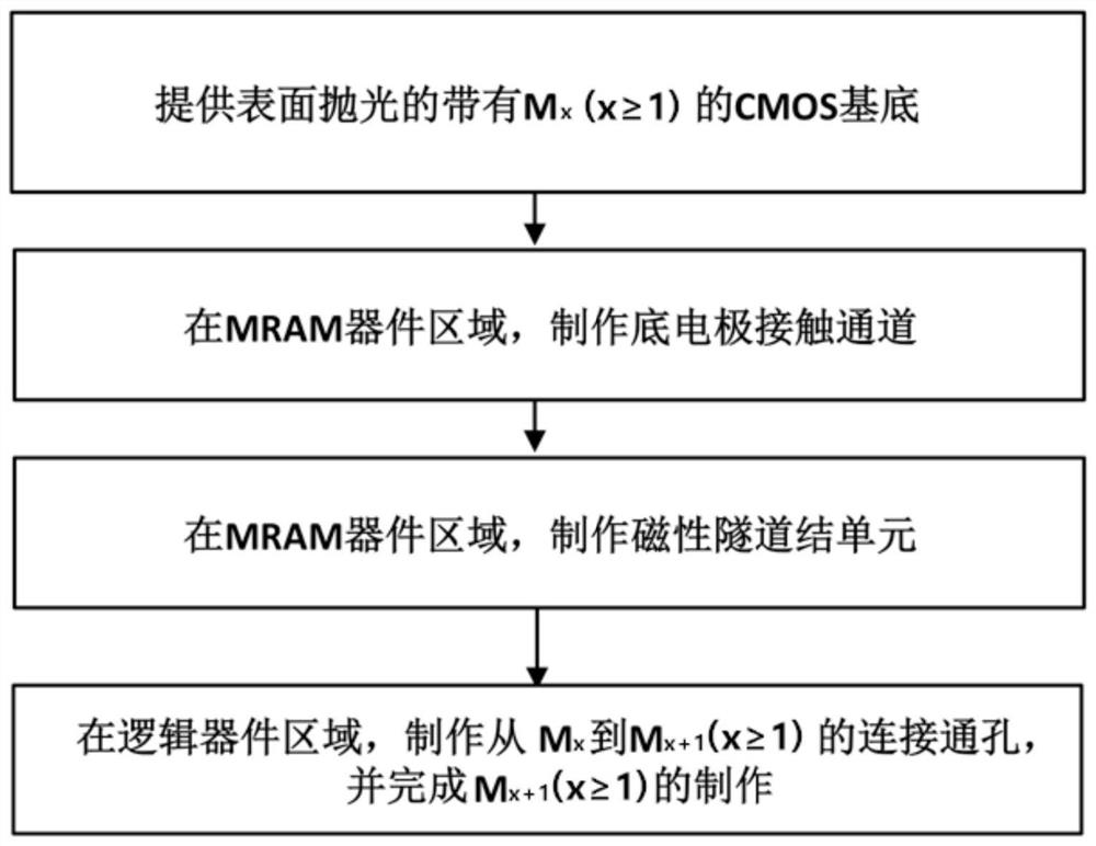
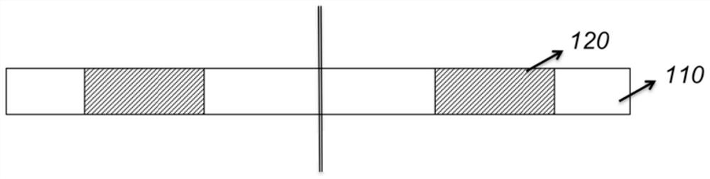
[0046] Symbols and indications in this embodiment:

[0047] m x (x≥1): the first metal connecting wire

[0048] m x+1 (x≥1): the second metal connecting wire

[0049] V x (x≥1): through hole

[0050] A kind of method of making magnetic random access memory provided by the present invention, by improving the connection method of magnetic tunnel junction and CMOS circuit, namely: in M x (x≥1) make tungsten or tantalum bottom electrode contact (BEC, Bottom Electrode Contact) instead of copper V x (x...


PUM

PropertyMeasurementUnit
thicknessaaaaaaaaaa
thicknessaaaaaaaaaa
thicknessaaaaaaaaaa

Abstract

The invention provides a method for making a magnetic random access memory, by improving the connection method between the magnetic tunnel junction and the CMOS circuit, that is: making a tungsten or tantalum bottom electrode contact (BEC, Bottom Electrode Contact) on the first metal connection line to replace copper Via hole; directly make the top electrode contact with the second metal connection line to replace the additional connection via hole (VIA), and at the same time, use the self-aligned etching process to complete the second metal connection line and logic device in the MRAM device area at one time Etching of the through hole and the second metal connection line in the area. The beneficial effect of the present invention is that the pollution problem caused by copper is avoided, and the complexity of the process and the production cost are reduced.

Description

technical field [0001] The present invention relates to a kind of method of making magnetic random access memory, be specifically related to a kind of two-layer CMOS metal connecting line (namely: M x and M x+1 (x≥1)) A method for fabricating a magnetic tunnel junction (MTJ, Magnetic Tunnel Junction) structural unit and its associated logic unit belongs to the field of magnetic random access memory (MRAM, Magnetic Radom Access Memory) manufacturing technology. Background technique [0002] In recent years, MRAM using magnetic tunnel junction (MTJ) has been considered as the future solid-state non-volatile memory, which has the characteristics of high-speed reading and writing, large capacity and low energy consumption. Ferromagnetic MTJ is usually a sandwich structure, which has a magnetic memory layer, which can change the magnetization direction to record different data; an insulating tunnel barrier layer in the middle; a magnetic reference layer, located on the other sid...

Claims


Application Information

Patent Timeline
Patent Type & Authority Patents(China)
IPC IPC(8): H01L43/14H10N52/01
CPCH10N52/01
Inventor 张云森
Owner SHANGHAI CIYU INFORMATION TECH CO LTD
Features
  • R&D
  • Intellectual Property
  • Life Sciences
  • Materials
  • Tech Scout
  • Unparalleled Data Quality
  • Higher Quality Content
  • 60% Fewer Hallucinations
Learn More