Single suspension beam gas sensor, sensor array and preparation method of sensor
A technology of gas sensor and cantilever beam, which is applied in the fields of MEMS and gas detection, can solve the problems of difficult positioning, low efficiency, complicated process, etc., and achieve the effects of easy preparation, improved production efficiency, and simple process
- Summary
- Abstract
- Description
- Claims
- Application Information
AI Technical Summary
Problems solved by technology
Method used
Image
Examples
Embodiment 1
[0059] A method for preparing a single cantilever gas sensor, comprising the following steps:
[0060] (1) Choose a silicon wafer with a crystal orientation of as the substrate, with a resistivity of 3-8Ωcm, a silicon wafer thickness of 350±10μm, and an angle error of trimming <1%;
[0061] (2) On the substrate, a layer with a thickness of of silicon oxide and a layer thickness of of silicon nitride;
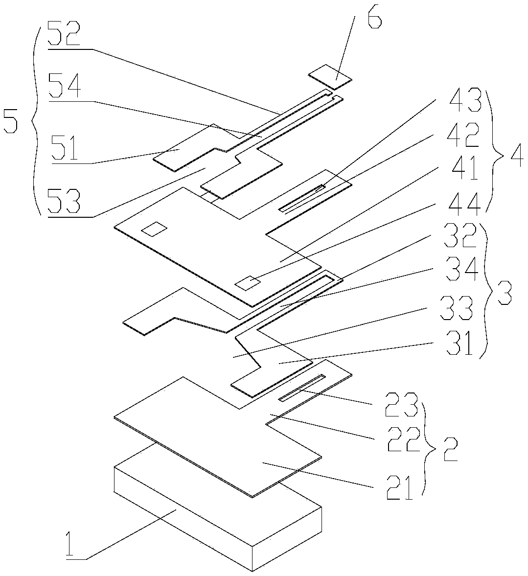
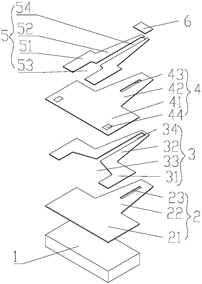
[0062] (3) Fabrication of heating resistor 3: The heating resistance wire of platinum resistance is produced by stripping process, with a thickness of
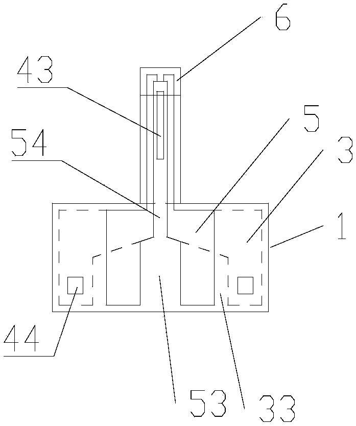
[0063] (4) Make isolation film 4: Utilize plasma enhanced chemical vapor deposition to make silicon oxide or silicon nitride as isolation film 4, the thickness of isolation film 4 is Then use reactive ion etching or ion beam etching to etch the isolation film 4 to form a through hole 44 to expose the heating resistor 3 below;
[0064] (5) make detecting electrode 5: utilize stripping process to make material be the det...
Embodiment 2
[0068] A method for preparing a single cantilever gas sensor, comprising the following steps:
[0069] (1) Take a silicon wafer as the substrate, its resistivity is 3-8Ωcm, the thickness of the silicon wafer is 350±10 μm, and the angle error of trimming is <1%;
[0070] (2) On the substrate, a layer with a thickness of of silicon oxide and a layer thickness of of silicon nitride;
[0071] (3) Fabrication of heating resistor 3: The heating resistance wire of platinum resistance is produced by stripping process, with a thickness of
[0072] (4) Make isolation film 4: Utilize plasma enhanced chemical vapor deposition to make silicon oxide or silicon nitride as isolation film 4, the thickness of isolation film 4 is Then use reactive ion etching or ion beam etching to etch the isolation film 4 to form a through hole 44 to expose the heating resistor 3 below;
[0073] (5) make detecting electrode 5: utilize stripping process to make material be the detecting electrode 5 of ...
Embodiment 3
[0077] A method for preparing a single cantilever gas sensor, comprising the following steps:
[0078] (1) Take a silicon wafer as the substrate, its resistivity is 3-8Ωcm, the thickness of the silicon wafer is 350±10 μm, and the angle error of trimming is <1%;
[0079] (2) On the substrate, a layer with a thickness of of silicon oxide and a layer thickness of of silicon nitride;
[0080] (3) Fabrication of heating resistor 3: The heating resistance wire of platinum resistance is produced by stripping process, with a thickness of
[0081] (4) Make isolation film 4: Utilize plasma enhanced chemical vapor deposition to make silicon oxide or silicon nitride as isolation film 4, the thickness of isolation film 4 is Then use reactive ion etching or ion beam etching to etch the isolation film 4 to expose the heating resistor 3 below;
[0082] (5) make detecting electrode 5: utilize stripping process to make material be the detecting electrode 5 of platinum, thickness is ...
PUM
| Property | Measurement | Unit |
|---|---|---|
| Resistivity | aaaaa | aaaaa |
Abstract
Description
Claims
Application Information


