
A kind of preparation method of nanostructure silicon negative electrode material

A silicon negative electrode, nano-micro technology, applied in structural parts, electrode manufacturing, nanotechnology for materials and surface science, etc., can solve the problem that the pore size distribution of porous silicon negative electrode materials is difficult to control, and high volume specific capacity batteries are difficult to achieve. For the first time, The problem of low coulombic efficiency in charge and discharge can achieve excellent cycle performance, inhibit volume expansion, and improve cycle performance.

Active Publication Date: 2020-12-04
湖南宸星新材料研究院有限公司
View PDF5 Cites 0 Cited by
  • Summary
  • Abstract
  • Description
  • Claims
  • Application Information

AI Technical Summary

Problems solved by technology

The difficulty in preparing porous silicon anode materials is that its pore size distribution is difficult to control
Due to the large specific surface area of ​​porous silicon materials, the coulombic efficiency of the first charge and discharge is low, and the tap density is low, making it difficult to achieve high volume specific capacity batteries

Method used


Image

  • A kind of preparation method of nanostructure silicon negative electrode material
  • A kind of preparation method of nanostructure silicon negative electrode material
  • A kind of preparation method of nanostructure silicon negative electrode material

Examples


Embodiment 1

[0042] A kind of preparation method of nanostructure silicon negative electrode material of the present invention, comprises the steps:

[0043] (1) Disperse metallurgical-grade micro-silicon in a 5% ethanol dispersion and disperse it ultrasonically for 10 minutes to obtain a silicon pre-dispersion;

[0044] (2) Take HF-AgNO 3 solution system. HF concentration is 5mol / L, AgNO 3 The concentration is 0.01mol / L, and the etchant is slowly added into the silicon pre-dispersion liquid through a peristaltic pump at 10ml / min, and the reaction is carried out for 5 minutes, and then suction filtered to obtain micron silicon with Ag particles deposited on the surface;

[0045] (3) redispersing the micron silicon with Ag particles deposited on the surface obtained in step (2) in a 5% ethanol dispersion, and stirring to obtain a silicon dispersion;

[0046] (4) HF-H 2 o 2 The solution is added into the silicon dispersion obtained in step (3) by a peristaltic pump at a speed of 10ml / mi...

Embodiment 2

[0053] A kind of preparation method of nanostructure silicon negative electrode material of the present invention, comprises the steps:

[0054] (1) Disperse metallurgical-grade micro-silicon in a 5% ethanol dispersion and disperse it ultrasonically for 10 minutes to obtain a silicon pre-dispersion;

[0055] (2) Take HF-AgNO 3 Solution system, HF concentration is 5mol / L, AgNO 3 The concentration is 0.005mol / L, and the etchant is slowly added to the silicon pre-dispersion liquid through a peristaltic pump at 10ml / min, and the reaction is carried out for 5 minutes, and then suction filtered to obtain micron silicon with Ag particles deposited on the surface;

[0056] (3) redispersing the micron silicon with Ag particles deposited on the surface obtained in step (2) in a 5% ethanol dispersion, and stirring to obtain a silicon dispersion;

[0057] (4) HF-H 2 o 2 The solution is added into the silicon dispersion obtained in step (3) by a peristaltic pump at a speed of 10ml / min,...

Embodiment 3

[0062] A kind of preparation method of nanostructure silicon negative electrode material of the present invention, comprises the steps:

[0063] (1) Disperse metallurgical-grade micro-silicon in a 5% ethanol dispersion and disperse it ultrasonically for 10 minutes to obtain a silicon pre-dispersion;

[0064] (2) Take HF-AgNO 3 Solution system, HF concentration is 5mol / L, AgNO 3 The concentration is 0.02mol / L, and the etchant is slowly added into the silicon pre-dispersion liquid through a peristaltic pump at 10ml / min, and the reaction is carried out for 5 minutes, and then suction filtered to obtain micron silicon with Ag particles deposited on the surface;

[0065] (3) Redisperse the micron silicon with Ag particles deposited on the surface in 5% ethanol dispersion, and obtain the dispersion of silicon after stirring;

[0066] (4) HF-H 2 o 2 The solution is added into the silicon dispersion obtained in step (3) by a peristaltic pump at a speed of 10ml / min, the HF concentr...


PUM

PropertyMeasurementUnit
particle sizeaaaaaaaaaa
pore sizeaaaaaaaaaa
particle diameteraaaaaaaaaa

Abstract

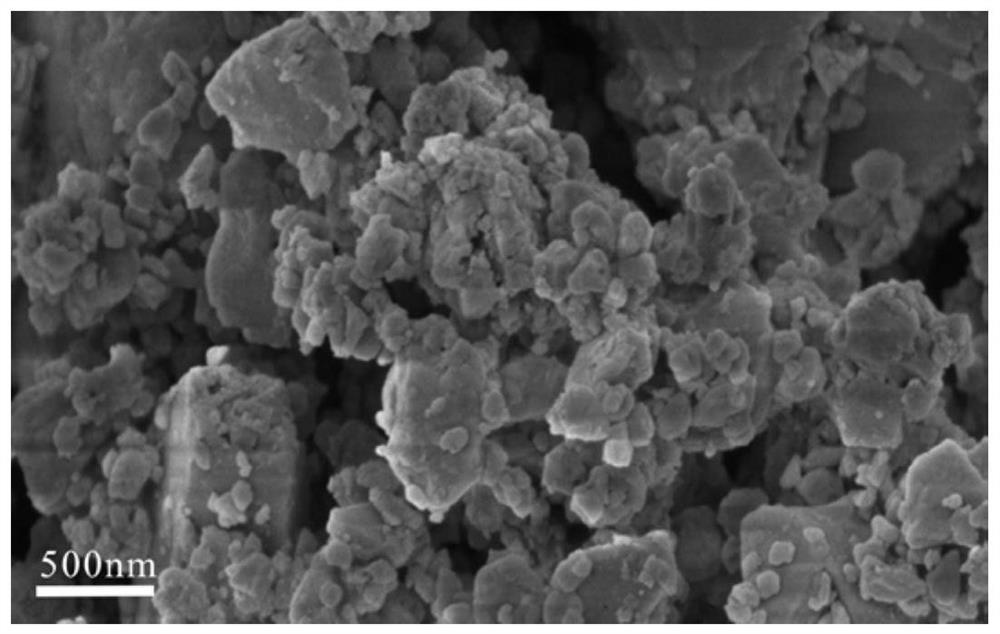
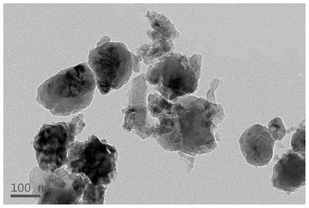
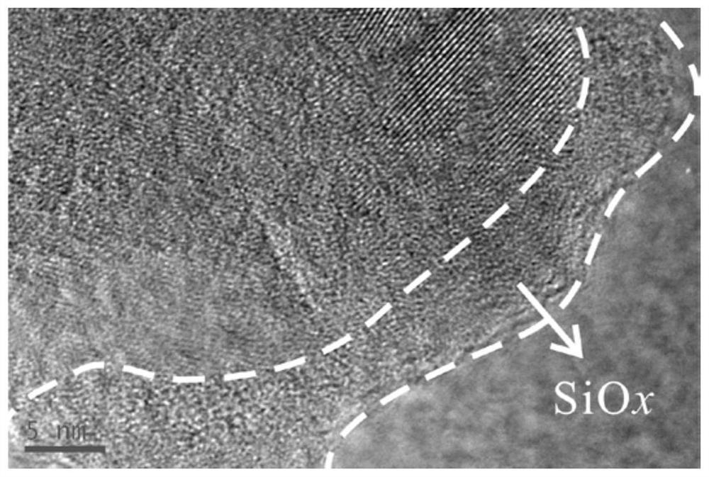
The invention discloses a nano microstructure silicon negative electrode material preparation method. The preparation method comprises the following steps: 1) metallurgy nano silicon is dispersed in organic dispersion liquid; 2) HF-metal salting liquid is prepared as an etching agent, the etching agent is slowly added in silicon pre-dispersion liquid, and the nano silicon with the surface deposited with the metal particles can be obtained; 3) the nano silicon with the surface deposited with the metal particles is re-dispersed in the organic dispersion liquid; 4) a HF-H2O2 solution is added inthe silicon dispersion liquid, and the organic dispersion liquid is intermittently added; 5) porous silicon is immersed in a HNO3 solution to obtain the high-purity porous silicon; and 6) the high-purity porous silicon is subjected to ball milling processing with a controllable oxidation degree. The method employs combination of metal auxiliary chemical etching and ball milling with the controllable oxidation degree, and the nano microstructure silicon negative electrode material with the surface coated with a layer of compact oxide SiOx and having micropores inside can be prepared, a lithium ion transmission path is shortened, silicon volume expansion can be accommodated, and the method has excellent cycle stability.

Description

technical field [0001] The invention belongs to the technical field of porous nanometer functional materials, and relates to a preparation method of silicon negative electrode material with nanostructure and microstructure. Background technique [0002] As an energy storage device, lithium-ion batteries have the advantages of high energy density, good cycle performance, and environmental protection, and are widely used in portable electronic devices such as mobile phones, notebook computers, game consoles, and unmanned aircraft. In recent years, my country has vigorously developed new energy vehicles and energy storage industries, and there is an urgent need to develop battery anode materials with higher specific capacity and low cost. Silicon has the potential to replace graphite as the anode material for the next generation of high-energy lithium-ion batteries due to its high theoretical specific capacity, low lithium intercalation potential, and wide range of sources. Ho...

Claims


Application Information

Patent Timeline
Patent Type & Authority Patents(China)
IPC IPC(8): H01M4/38H01M10/0525H01M4/04C01B33/021B82Y30/00B82Y40/00
CPCB82Y30/00B82Y40/00C01B33/021H01M4/0402H01M4/38H01M10/0525Y02E60/10
Inventor 杨娟陈松唐晶晶周向阳张佳明任永鹏于亚文
Owner 湖南宸星新材料研究院有限公司
Learn More