Solar cell having a plurality of absorbers connected to one another by means of charge-carrier-selective contacts
A technology of solar cells and absorbers, applied in the field of solar cells, can solve problems such as degradation and achieve the effect of minimizing electrical loss
- Summary
- Abstract
- Description
- Claims
- Application Information
AI Technical Summary
Problems solved by technology
Method used
Image
Examples
Embodiment Construction
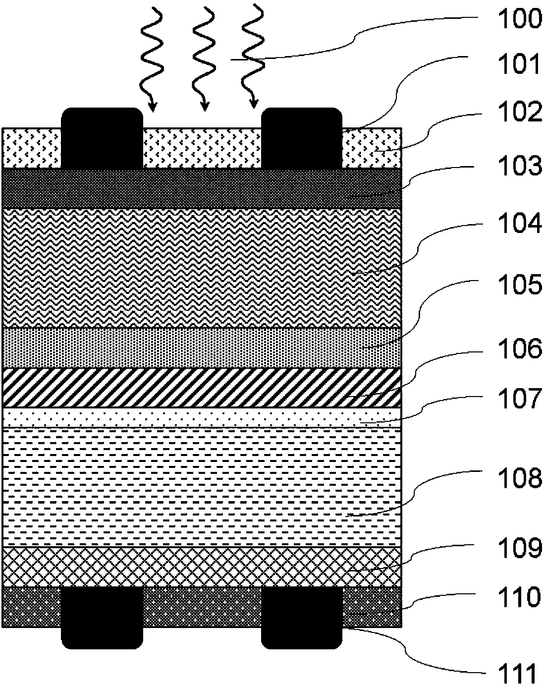
[0033] figure 1 A schematic diagram showing a tandem solar cell according to the first of two preferred embodiments of the present invention.
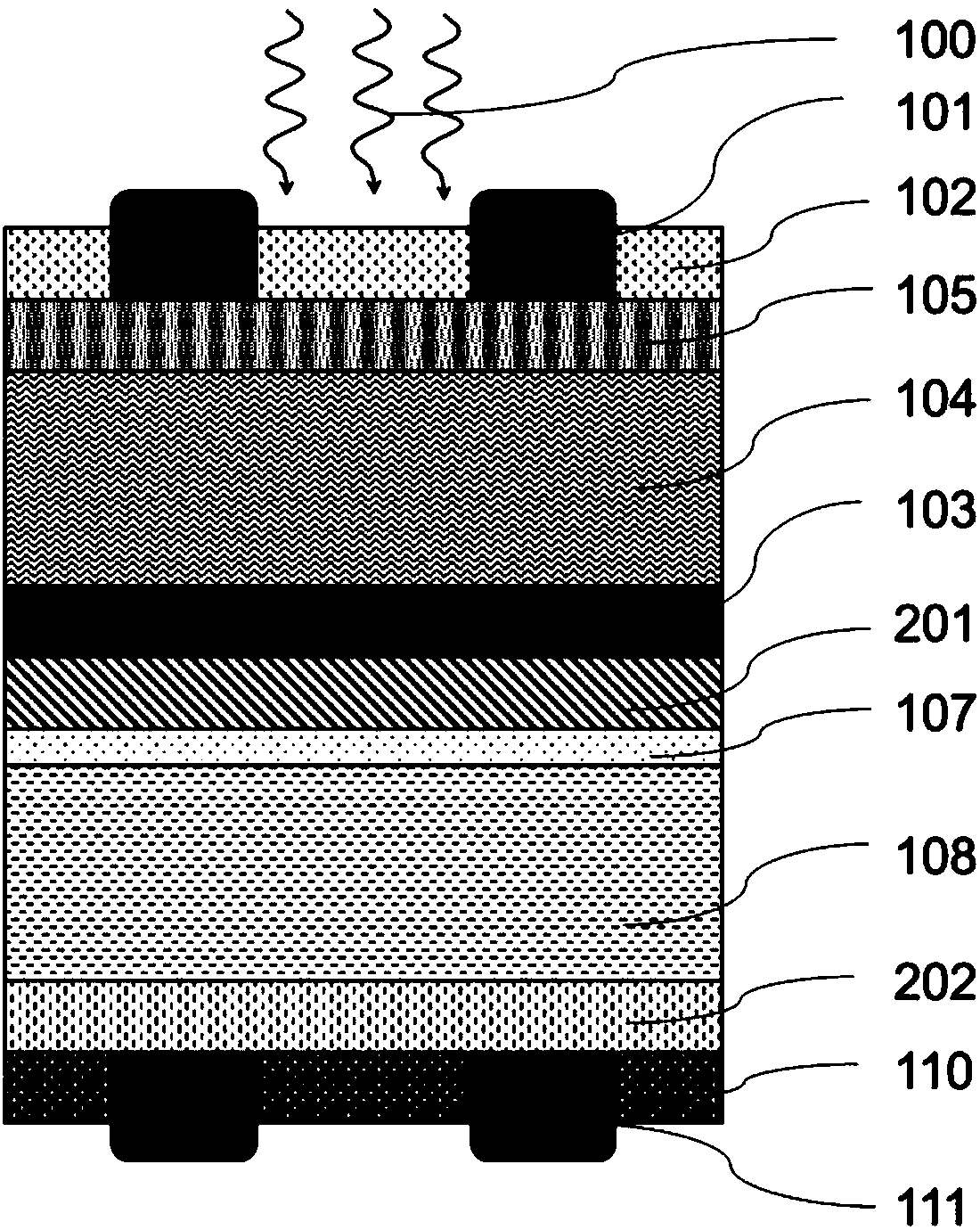
[0034] Such as figure 1 As shown, the tandem solar cell has two different absorbers 104, 108 made of different materials. Alternatively, more than three different absorbent body materials may be used. In either case, according to the invention, the first absorber is made of silicon ( figure 1 108 in).
[0035] The silicon absorber 108 can be, for example, a wafer made of crystalline silicon, in particular monocrystalline or polycrystalline silicon. Saw damage is removed from the surface of the silicon absorber 108 if necessary. The thickness of the silicon absorber 108 is generally in the range of 30-500 μm, preferably 50-300 μm. The horizontal size is usually 0.1×0.1cm 2 up to 200×200cm 2 In the range. The silicon absorber 108 can be p-doped, n-doped or undoped or intrinsic. The silicon absorber 108 preferably has the same d...
PUM
 Abstract
Description
Claims
Application Information
 - R&D
- Intellectual Property
- Life Sciences
- Materials
- Tech Scout
- Unparalleled Data Quality
- Higher Quality Content
- 60% Fewer Hallucinations
Browse by: Latest US Patents, China's latest patents, Technical Efficacy Thesaurus, Application Domain, Technology Topic, Popular Technical Reports.
© 2025 PatSnap. All rights reserved.Legal|Privacy policy|Modern Slavery Act Transparency Statement|Sitemap|About US| Contact US: help@patsnap.com


