Gas concentration and sensing integrated device and preparation method thereof

A gas sensor and concentrator technology, applied in the field of integrated devices and preparation, can solve the problems of long thermal relaxation time of the acetone sensor and the gas concentrator, weakening the concentration effect of the gas concentrator, unable to integrate intelligent terminals, etc., so as to shorten the thermal relaxation time. The effect of hemp time, reduction of size and power consumption, and scientific preparation method

Active Publication Date: 2018-08-07
HEFEI INSTITUTES OF PHYSICAL SCIENCE - CHINESE ACAD OF SCI
View PDF13 Cites 3 Cited by
  • Summary
  • Abstract
  • Description
  • Claims
  • Application Information

AI Technical Summary

Problems solved by technology

Although this kind of monitoring sensor can be used for the detection of trace acetone gas, it also has shortcomings. First, it is bulky, and the volume of the glass bottle for placing the whole set of concentrated measurement devices is as high as 16.9ml, which cannot be integrated into smart terminals such as mobile phones; secondly, , the distance between the acetone sensor and the gas concentrator is relatively long, on the order of centimeters, which seriously weakens the concentration effect of the gas concentrator; again, the volume of the platinum heating wire for heating the zeolite gas concentrator is too large—300×300×500 μm 3 , not only lead to a large power consumption of the platinum heating wire, but also cause a longer thermal relaxation time of the acetone sensor and the gas concentrator, which is not conducive to rapid sampling testing

Method used


Image

  • Gas concentration and sensing integrated device and preparation method thereof
  • Gas concentration and sensing integrated device and preparation method thereof

Examples


Embodiment 1

[0045] The concrete steps of preparation are:

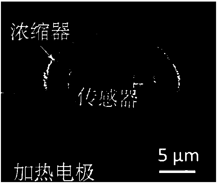
[0046] Step 1, after coating an electron beam resist on the silicon wafer covered with a mesoporous thermal insulation layer, a sensor pattern with a length of 3 μm and a width of 1.5 μm is drawn on it by an electron beam exposure method; wherein, The e-beam resist was ZEP 520A e-beam resist. After the metal oxide gas sensor is sputtered on the sensor pattern by magnetron sputtering, it is placed in dimethylformamide solution to peel off the electron beam resist to obtain the surface covered with the metal oxide gas sensor A silicon wafer covered with a mesoporous heat-insulating layer; wherein, the sputtering power of the metal oxide gas sensor is 80W and the sputtering time is 60min when using the magnetron sputtering method, and the thickness of the metal oxide gas sensor is 200nm. The metal oxide is tin dioxide.

[0047] Step 2, after the electron beam resist is coated on the silicon wafer covered with the mesoporous heat i...

Embodiment 2

[0052] The concrete steps of preparation are:

[0053] Step 1, after coating an electron beam resist on the silicon wafer covered with a mesoporous thermal insulation layer, a sensor pattern with a length of 3.5 μm and a width of 1.2 μm is drawn on it by an electron beam exposure method; , the electron beam resist is ZEP 520A electron beam resist. After the metal oxide gas sensor is sputtered on the sensor pattern by magnetron sputtering, it is placed in dimethylformamide solution to peel off the electron beam resist to obtain the surface covered with the metal oxide gas sensor A silicon wafer covered with a mesoporous heat-insulating layer; wherein, the sputtering power of the metal oxide gas sensor is 90W, the sputtering time is 48min, and the thickness of the metal oxide gas sensor is 175nm when using the magnetron sputtering method. The metal oxide is tin dioxide.

[0054] Step 2, after the electron beam resist is coated on the silicon wafer covered with the mesoporous h...

Embodiment 3

[0059] The concrete steps of preparation are:

[0060] Step 1, after coating an electron beam resist on the silicon wafer covered with a mesoporous thermal insulation layer, a sensor pattern with a length of 4 μm and a width of 0.9 μm is drawn on it by an electron beam exposure method; wherein, The e-beam resist was ZEP 520A e-beam resist. After the metal oxide gas sensor is sputtered on the sensor pattern by magnetron sputtering, it is placed in dimethylformamide solution to peel off the electron beam resist to obtain the surface covered with the metal oxide gas sensor A silicon wafer covered with a mesoporous heat-insulating layer; wherein, the sputtering power of the metal oxide gas sensor is 100W and the sputtering time is 35min when using the magnetron sputtering method, and the thickness of the metal oxide gas sensor is 150nm. The metal oxide is tin dioxide.

[0061] Step 2, after the electron beam resist is coated on the silicon wafer covered with the mesoporous heat ...


PUM

PropertyMeasurementUnit
thicknessaaaaaaaaaa

Abstract

The invention discloses a gas concentration and sensing integrated device and a preparation method thereof. The integrated device comprises a metal-oxide gas sensor, an annular insulating layer, an annular platinum micro-heater, an annular insulating layer and an annular gas concentrator which are successively placed on a silicon wafer and are connected with an electrode, a mesoporous heat-insulation layer covers the silicon wafer, the width of the annular platinum micro-heater is less than or equal to 1 mu m, the thickness is 200-500 nm, and the electrode is electrically connected with the platinum micro-heater and a power supply separately. The method comprises the following steps: repeatedly coating the silicon wafer covered with the mesoporous heat-insulation layer with an electron beam resist; drawing a graph of a corresponding device on the electron beam resist through an electron beam exposure method; and after sputtering or evaporating the corresponding device on the graph, growing the gas concentrator on the annular insulating layer to obtain a target product. The gas concentration and sensing integrated device has the advantages of compact structure, low power consumption, high detection limit, instantaneity and convenience, is quite easily applied to high-sensitivity detection on gas widely, and thus has a wide application prospect in the fields of wearable or embeddable intelligent terminals and the like.

Description

technical field [0001] The invention relates to an integrated device and a preparation method, in particular to a gas concentration and sensing integrated device and a preparation method thereof. Background technique [0002] Trace gases in indoor and outdoor environments carry important information related to the environment and health. The development of wearable or embedded smart terminal micro-semiconductor gas sensors will be at the forefront of the development of the Internet of Things era and has broad market application prospects. Recently, in order to further improve the detection limit of oxide semiconductor gas sensors, so as to effectively promote its application in the fields of trace pollution gas and respiratory gas detection, some beneficial attempts and efforts have been made, such as the title "UItratrace Measurement of Acetone from Skin Using Zeol ite: Toward Development of a Wearable Monitor of Fat Metabolism", Analytical Chemistry, 87(2015) 7588-7594 , ...

Claims


Application Information

Patent Timeline
Patent Type & Authority Applications(China)
IPC IPC(8): G01N1/40G01N27/00
CPCG01N1/40G01N27/00
Inventor 孟钢方晓东邓赞红邵景珍
Owner HEFEI INSTITUTES OF PHYSICAL SCIENCE - CHINESE ACAD OF SCI
Why Eureka
Try Eureka