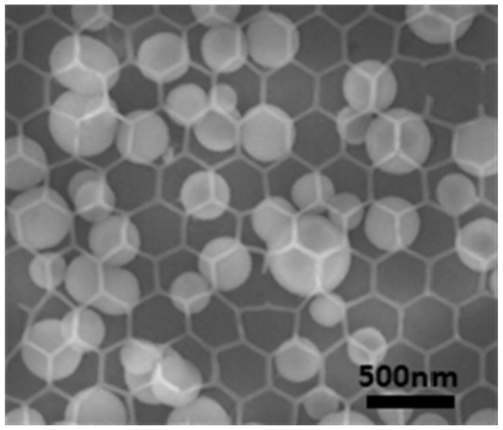
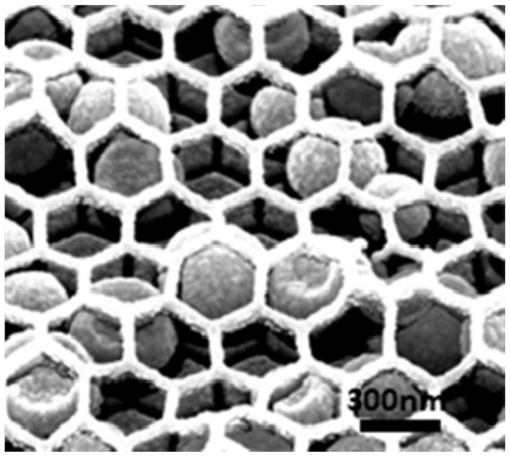
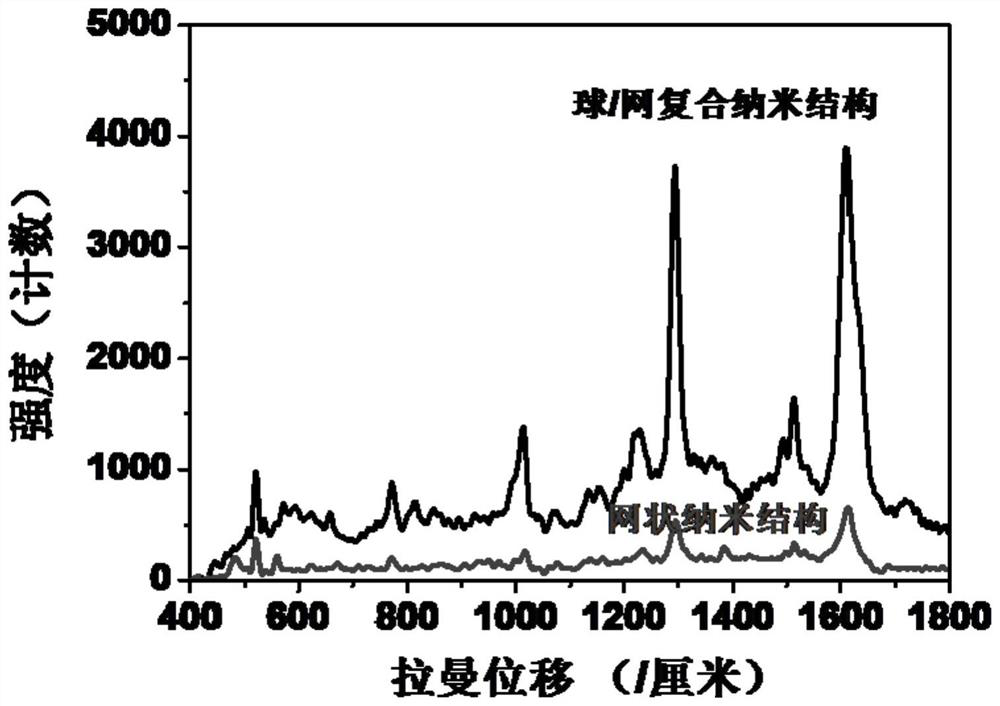
A surface-enhanced Raman substrate and its preparation method
A substrate and substrate technology, applied in the field of surface-enhanced Raman substrate and its preparation
- Summary
- Abstract
- Description
- Claims
- Application Information
AI Technical Summary
Problems solved by technology
Method used
Image
Examples
Embodiment 1
[0087] This embodiment provides a method for preparing a surface-enhanced Raman substrate, the specific method of which is:
[0088] (1) Clean the silicon (100) substrate, mix the negative electron beam resist HSQ and the positive electron beam resist PMMA 950k according to the volume ratio of 1:1, and ultrasonically disperse the mixed resist solution for 30 minutes. The e-beam resist was spin-coated to a thickness of 250 nm on a silicon substrate to obtain a coated substrate.
[0089] (2) On the coated substrate described in step (1), use an electron beam with a beam spot diameter of 6 nm to expose the electron beam resist, and adjust the exposure dose to 190000 μC / cm 2 The hexagonal nano-array pattern is directly written to obtain a substrate on which the nano-array pattern is written. The area of the nano-array pattern is 150 μm×150 μm, and the layout design line width of the nano-array pattern is 6 nm.
[0090] (3) Develop the substrate written in the nanoarray pattern ...
Embodiment 2
[0098] This embodiment provides a method for preparing a surface-enhanced Raman substrate, the specific method of which is:
[0099] (1) Clean the silicon (100) substrate, mix the negative electron beam resist HSQ and the positive electron beam resist ZEP520 according to the volume ratio of 3:2, ultrasonically disperse the mixed resist solution for 5 minutes, and The e-beam resist was spin-coated to a thickness of 400 nm on a silicon substrate to obtain a coated substrate.
[0100] (2) On the coated substrate described in step (1), use an electron beam with a beam spot diameter of 4 nm to expose the electron beam resist, and adjust the exposure dose to 120000 μC / cm 2 The hexagonal nano-array pattern is directly written to obtain a substrate on which the nano-array pattern is written. The area of the nano-array pattern is 250 μm×250 μm, and the layout design line width of the nano-array pattern is 4 nm.
[0101] (3) Develop the substrate written in the nanoarray pattern desc...
Embodiment 3
[0107] This embodiment provides a method for preparing a surface-enhanced Raman substrate, the specific method of which is:
[0108] (1) Clean the silicon (100) substrate, mix the negative electron beam resist HSQ and the positive electron beam resist PMMA 950k according to the volume ratio of 1:3, and ultrasonically disperse the mixed resist solution for 2 minutes, The e-beam resist was spin-coated to a thickness of 4800 nm on a silicon substrate to obtain a coated substrate.
[0109] (2) On the coated substrate described in step (1), use an electron beam with a beam spot diameter of 1 nm to expose the electron beam resist, and adjust the exposure dose to 200000 μC / cm 2 The triangular nano-array pattern is directly written to obtain a base on which the nano-array pattern is written. The area of the nano-array pattern is 10 μm×10 μm, and the layout design line width of the nano-array pattern is 1 nm.
[0110] (3) Develop the substrate written in the nanoarray pattern descri...
PUM
| Property | Measurement | Unit |
|---|---|---|
| width | aaaaa | aaaaa |
| diameter | aaaaa | aaaaa |
| thickness | aaaaa | aaaaa |
Abstract
Description
Claims
Application Information
 - R&D Engineer
- R&D Manager
- IP Professional
- Industry Leading Data Capabilities
- Powerful AI technology
- Patent DNA Extraction
Browse by: Latest US Patents, China's latest patents, Technical Efficacy Thesaurus, Application Domain, Technology Topic, Popular Technical Reports.
© 2024 PatSnap. All rights reserved.Legal|Privacy policy|Modern Slavery Act Transparency Statement|Sitemap|About US| Contact US: help@patsnap.com


