Surface-enhanced Raman scattering (SERS) substrate and manufacturing method thereof
A surface-enhanced Raman and substrate technology, applied in the field of physics, can solve the problems of uncontrollable preparation process, complicated preparation process, and poor repeatability, and achieve the effects of controllable and uniform substrate, simple and efficient process, and low cost
- Summary
- Abstract
- Description
- Claims
- Application Information
AI Technical Summary
Problems solved by technology
Method used
Image
Examples
Embodiment 1
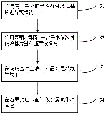
[0029] Such as figure 1 Shown, the preparation method of surface-enhanced Raman scattering substrate of the present invention, specific operation steps
[0030] as follows:
[0031] S1: Use an anionic surfactant, such as a dilute solution of fatty acid sodium (soapy water is also available), for stone
[0032] British glass substrates are pre-cleaned;
[0033] S2: Use acetone, alcohol, and deionized water to perform ultrasonic cleaning on the quartz glass substrate in order to remove
[0034] To remove surface oxides or impurities, the cleaning time is 5-20min, and the temperature is controlled at 0°C;
[0035] S3: Add graphene suspension dropwise on the quartz glass substrate, add 2 g of graphene powder into 40 ml of isopropanol (absolute ethanol is also available), and stir it into a uniform 0.08 g / ml Graphene suspension, drop 0.4 ml of graphene suspension onto the cleaned quartz glass substrate, and dry it in vacuum at 40°C to form a graphene layer on the quartz glass;...
Embodiment 2
[0041] This embodiment specifically describes the surface-enhanced Raman scattering substrate of the present invention, which includes: a glass substrate,
[0042] Graphene (Graphene) layer and metal oxide film layer.
[0043] In this embodiment, the graphene layer is located on the upper surface of the glass substrate, and the metal oxide film layer is located on the upper surface of the graphene layer.
[0044] In this embodiment, the glass substrate is a quartz glass substrate.
[0045] In this embodiment, the metal oxide film layer is a cuprous oxide layer.
[0046] In a preferred embodiment, the glass substrate can be K9 glass, quartz or crystal.
Embodiment 3
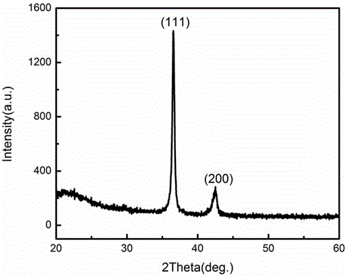
[0048] On the basis of Example 1, this embodiment is used to test the X-ray diffraction pattern of the obtained cuprous oxide film layer of the surface-enhanced Raman scattering substrate having a graphene layer.
[0049] In this embodiment, the test of the X-ray diffraction spectrum of the cuprous oxide film layer is used to detect whether the cuprous oxide is oxidized, that is, to ensure the quality and good crystallinity of the cuprous oxide film layer, and to ensure that the surface-enhanced pulley prepared by the present invention The excellent quality of the Mann scattering substrate.
[0050] Such as figure 2 As shown, the X-ray diffraction spectrum of the cuprous oxide film layer that the present embodiment obtains, wherein, (111), (200) are respectively two crystal planes of cuprous oxide, (111) diffraction peak is narrow and peak height, It shows that the prepared cuprous oxide film layer has good quality and crystallinity, and can meet the requirements of the surf...
PUM
| Property | Measurement | Unit |
|---|---|---|
| concentration | aaaaa | aaaaa |
Abstract
Description
Claims
Application Information
 - R&D Engineer
- R&D Manager
- IP Professional
- Industry Leading Data Capabilities
- Powerful AI technology
- Patent DNA Extraction
Browse by: Latest US Patents, China's latest patents, Technical Efficacy Thesaurus, Application Domain, Technology Topic, Popular Technical Reports.
© 2024 PatSnap. All rights reserved.Legal|Privacy policy|Modern Slavery Act Transparency Statement|Sitemap|About US| Contact US: help@patsnap.com


