Supercharge Your Innovation With Domain-Expert AI Agents!

Transverse superjunction structure gallium nitride HEMT device and manufacturing method thereof

A manufacturing method and technology of gallium nitride, applied in semiconductor/solid-state device manufacturing, semiconductor devices, electrical components, etc., can solve the problems of device self-heating effect, two-dimensional electron gas scattering, uneven electric field distribution in the drift region, etc. The effect of breakdown voltage, reduction of lateral scattering, reduction of self-heating effects

Inactive Publication Date: 2018-08-24
CHONGQING UNIV
View PDF12 Cites 0 Cited by
  • Summary
  • Abstract
  • Description
  • Claims
  • Application Information

AI Technical Summary

Problems solved by technology

[0003] However, as a new generation of power devices, GaN HEMT devices have many problems in their performance
The most important point is that due to the high electric field concentration at the edge near the drain direction under the Schottky gate, the electric field distribution in the drift region is uneven, resulting in premature breakdown. The breakdown voltage of GaN HEMT devices Far from reaching the theoretical limit of GaN materials
At the same time, due to its large current, the two-dimensional electron gas has lateral electron scattering, which will cause serious self-heating effects inside the device.

Method used


Image

  • Transverse superjunction structure gallium nitride HEMT device and manufacturing method thereof
  • Transverse superjunction structure gallium nitride HEMT device and manufacturing method thereof
  • Transverse superjunction structure gallium nitride HEMT device and manufacturing method thereof

Examples


Embodiment Construction

[0039] The preferred embodiments of the present invention will be described in detail below with reference to the accompanying drawings.

[0040] Such as Figure 1-8 Shown, the inventive method comprises the steps:

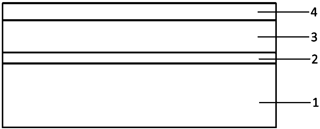
[0041] Step 1. If figure 1 As shown, a 300nm AlN layer 2, a 2μm GaN buffer layer 3, and a 100nm GaN channel layer 4 are epitaxially grown on a prepared silicon substrate 1 by PECVD (Plasma Enhanced Chemical Vapor Deposition) in sequence.

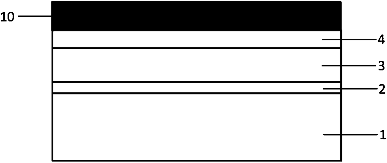
[0042] Step 2. coat a thick photoresist 10 on the epitaxial wafer obtained in step S1 as an ion implantation barrier such as figure 2 As shown, the photoresist thickness is 1 μm.

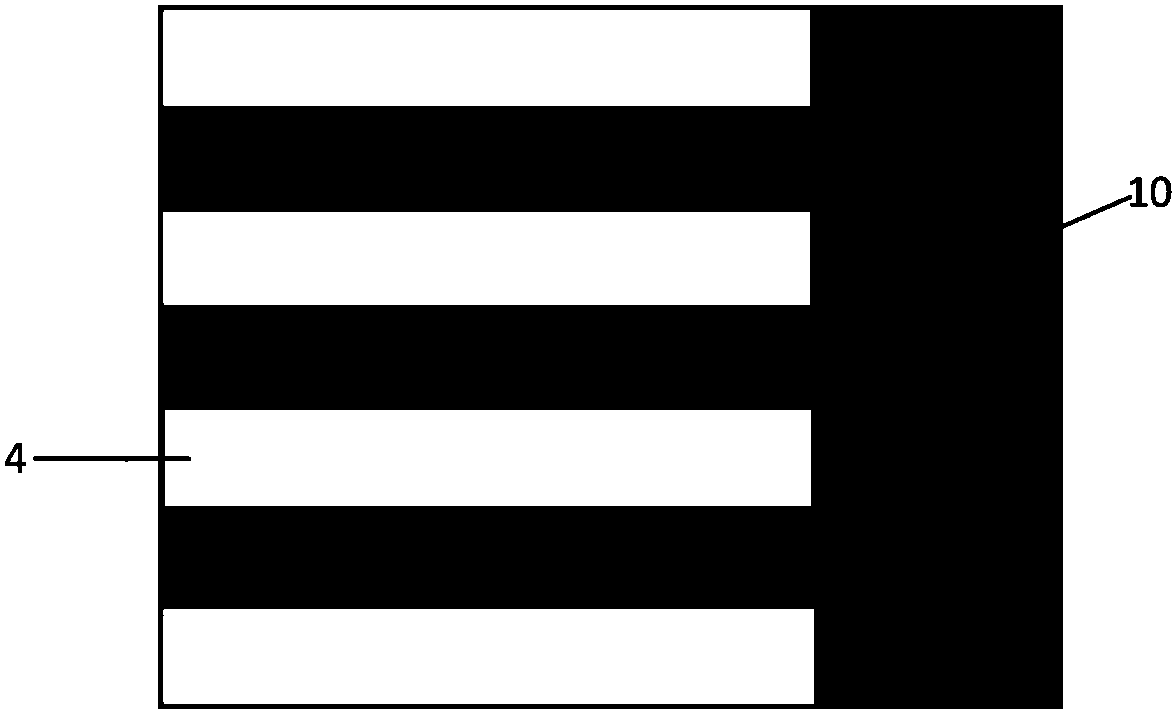
[0043] Step 3. Expose and develop the photoresist, such as image 3 As shown, the region of the GaN channel layer 4 that needs to be doped is exposed.

[0044] Step 4. Perform Mg ion implantation to form periodically spaced strip-shaped P-type doped regions 9 along the gate width direction in the GaN channel layer 4, such as Figure 4 and 5 A...


PUM

PropertyMeasurementUnit
Thicknessaaaaaaaaaa
Thicknessaaaaaaaaaa
Thicknessaaaaaaaaaa

Abstract

The invention relates to a transverse superjunction structure gallium nitride HEMT device and a manufacturing method thereof. The method comprises the following steps of S1, successively arranging anAlN layer, a GaN buffer layer, a GaN channel layer on a prepared substrate layer; S2, coating a layer of photoresist as an ion implantation barrier layer on an epitaxial wafer obtained in step S1; S3,exposing and developing the photoresist to expose the GaN channel layer requiring a doped region; S4, carrying out Mg ion implantation, and forming long-strip-type P-type doped regions which are arranged at periodic intervals along the plane direction of the GaN channel layer in the GaN channel layer; S5, removing the remaining photoresist, carrying out rapid thermal processing and activating doping ions; S6, arranging an AlGaN barrier layer; S7, cleaning the epitaxial wafer and using an ion implantation or plasma etching method to isolate devices so as to form the active region of the HEMT device; S8, making source and drain electrodes and forming ohmic contact; and S9, making a gate electrode and forming Schottky contact. In the invention, the breakdown voltage of the gallium nitride HEMT device is effectively increased.

Description

technical field [0001] The invention belongs to the technical field of power electronic devices, and relates to a gallium nitride HEMT device with a lateral superjunction structure and a manufacturing method thereof. Background technique [0002] With the development of microelectronics technology, the performance of traditional Si and GaAs semiconductor devices is close to the theoretical limit determined by the material itself. In recent years, gallium nitride (GaN), which is called the third-generation semiconductor with excellent high temperature, ) material has become a research hotspot in the world. The wide bandgap semiconductor GaN material has an ultra-high critical breakdown electric field, which is nearly 10 times higher than that of silicon (Si), and the heterojunction composed of AlGaN and GaN has a strong two-dimensional electron gas. Therefore, the on-resistance of AlGaN / GaN HEMT power devices is nearly three orders of magnitude lower than that of Si devices ...

Claims


Application Information

Patent Timeline
IPC IPC(8): H01L21/335H01L29/06H01L29/778
CPCH01L29/063H01L29/66462H01L29/7787
Inventor 陈显平肖霞叶怀宇王黎明王少刚檀春健罗厚彩
Owner CHONGQING UNIV
Features
  • R&D
  • Intellectual Property
  • Life Sciences
  • Materials
  • Tech Scout
  • Unparalleled Data Quality
  • Higher Quality Content
  • 60% Fewer Hallucinations
Learn More