

Topological insulator structure with insulating protective layer and preparation method thereof
A technology of topological insulator and insulating protective layer, which is applied in the field of topological insulator structure and its preparation, and can solve the problems of slow deposition rate and so on
- Summary
- Abstract
- Description
- Claims
- Application Information
AI Technical Summary
Problems solved by technology
Method used
Image

Examples
preparation example Construction
[0048] see Figure 4 , the present invention also provides a method for preparing the topological insulator structure with the insulating protection layer 30, comprising:
[0049]S100, providing the insulating substrate 10 in a molecular beam epitaxy reaction chamber;
[0050] S200, growing the topological insulator quantum well thin film 20 on the surface of the insulating substrate 10 having a first temperature by molecular beam epitaxy; and
[0051] S300, growing the insulating protective layer 30 on the surface of the topological insulator quantum well film 20 with the second temperature by molecular beam epitaxy.
[0052] In step S100, the insulating substrate 10 has an atomically flat surface. When the insulating substrate 10 is STO, specifically, the STO substrate can be cut out of the surface of the (111) crystal plane, heated in deionized water less than 100°C (such as 70°C), and heated in an atmosphere of oxygen and argon. Burn at 800°C to 1200°C (such as 1000°C)....
Embodiment 1
[0097] For analysis of surface topography and RHEED streaks on grown samples, see Figure 7 . (a) (b) (c) are respectively magnetic doping topological insulator quantum well film 20, the magnetic doping topological insulator quantum well film 20 covering the CdSe insulating protection layer 30 of about 1nm, two layers of magnetic doping topological insulator quantum well Surface topography diagram of a 1 nm CdSe insulating spacer layer 40 sandwiched between the thin film 20 . (d)(e)(f) are their corresponding RHEED stripes respectively.
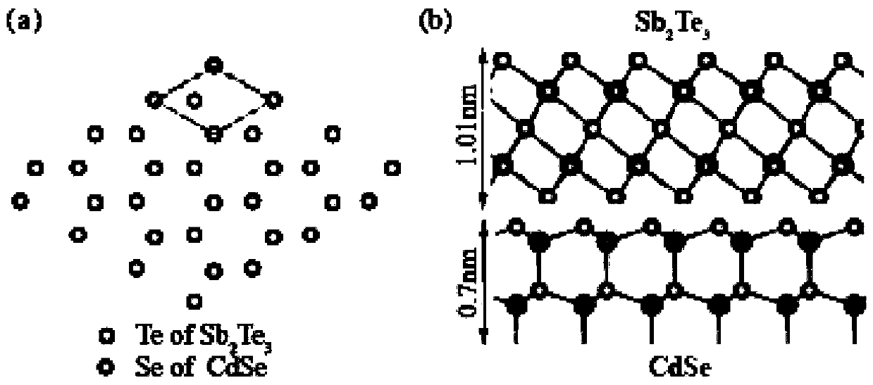
[0098] The comparison of (a) and (b) shows that after CdSe is grown on the magnetically doped topological insulator quantum well film 20, the surface morphology of the sample does not change substantially. From the comparison of (d) and (e) RHEED stripes, it can be seen that the lattice constant of the sample in the plane does not change basically after growing CdSe, indicating that they have a good lattice matching relationship. It can be...
Embodiment 2
[0100] TEM analysis of the lattice structure of a topological insulator with a CdSe insulating protective layer 30, see Figure 8 . (a) is the result of the superlattice structure formed by the magnetically doped topological insulator quantum well film 20 covering 4 layers of about 6QL and the CdSe protective layer of 3 layers of about 3.5nm, (b) is the result of the enlarged local range. It can be seen that the magnetically doped topological insulator quantum well thin film 20 and the CdSe protective layer have a good matching relationship of lattice epitaxial growth, forming a superlattice structure. The 6QL magnetically doped topological insulator quantum well film 20 can be well wrapped in the middle of the CdSe insulating protective layer 30 to form a capsule structure, which can form a good protective effect on the topological insulator.
PUM
 Abstract
Description
Claims
Application Information