

A preparing method for an inorganic halogen perovskite film
A technology of inorganic calcium and perovskite, which is applied in the direction of surface coating liquid devices, electrical components, coatings, etc., can solve the problem of insufficient density, small grain size, and the failure of inorganic perovskite films to meet the performance index requirements And other problems, to achieve excellent resistance to change performance, improve the effect of stability
- Summary
- Abstract
- Description
- Claims
- Application Information
AI Technical Summary
Problems solved by technology
Method used
Image


Examples
Embodiment 1
[0028] (1) Cleaning of the bottom electrode: Ultrasonic cleaning of the FTO conductive glass sheet (thickness about 1mm) with detergent for 20 minutes to remove organic and inorganic stains on the surface, then rinse with a large amount of tap water, and put the FTO conductive glass sheet into the Ultrasonic cleaning in deionized water for 20 minutes, followed by ultrasonic cleaning in absolute ethanol for 20 minutes to remove residual organic impurities on the surface, and this step was repeated several times. Afterwards, the FTO conductive glass sheet was ultrasonically cleaned in acetone for 20 minutes to further remove residual organic impurities on the surface. After cleaning with acetone, it was placed in a UV-ozone cleaner for 30 minutes. FTO is SnO doped with fluorine 2 Transparent conductive glass (SnO 2 : F).
[0029] (2) CsPbBr 3 Preparation of perovskite precursor storage solution: mix CsBr and PbBr at a molar ratio of 1:1 2 Dissolve in DMF, stir the reaction a...
Embodiment 2
[0035] (1) The cleaning of the bottom electrode is the same as in Example 1.
[0036] (2) CsPbBr 3 The preparation of the perovskite precursor storage solution is the same as in Example 1.
[0037] (3) spraying is the same as embodiment 1.
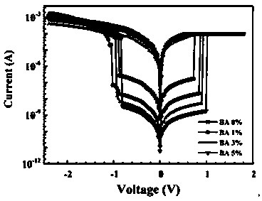
[0038] (4) Spin coating and annealing: transfer the above FTO substrate to a spin coater for spin coating (4000rpm ~ 1min), and continuously add 1mL of toluene and butyric acid mixed solvent on the perovskite layer during the spin coating process (wherein the content of butyric acid is 1%), and then place it on a heating plate at 250° C. for annealing for 10-15 minutes.
[0039] (5) Preparation of memristor storage unit by magnetron sputtering: place the perovskite film obtained above in a magnetron sputtering reaction chamber, and vacuumize to less than 5×10 -5Pa, high-purity argon gas was introduced as the working gas, the working pressure was 0.2Pa, the sputtering power was 65W, and the gold electrode with a thickness of about 300nm ...
Embodiment 3
[0042] (1) The cleaning of the bottom electrode is the same as in Example 1.
[0043] (2) CsPbBr 3 The preparation of the perovskite precursor storage solution is the same as in Example 1.
[0044] (3) spraying is the same as embodiment 1.
[0045] (4) Spin coating and annealing: transfer the above-mentioned FTO substrate to a spin coater for spin coating (1000rpm ~ 8s), and continuously drop 1mL of toluene and butyric acid mixed solvent on the perovskite layer during the spin coating process (wherein the content of butyric acid is 3%), and then place it on a heating plate at 250° C. for annealing for 10 to 15 minutes.
[0046] (5) Preparation of memristor storage unit by magnetron sputtering: place the perovskite film obtained above in a magnetron sputtering reaction chamber, and vacuumize to less than 5×10 -5 Pa, high-purity argon gas was introduced as the working gas, the working pressure was 0.2Pa, the sputtering power was 65W, and the gold electrode with a thickness of...
PUM
| Property | Measurement | Unit |
|---|---|---|
| Thickness | aaaaa | aaaaa |
Abstract
Description
Claims
Application Information