Planar LED epitaxial structure based on gallium arsenide substrate and manufacturing method thereof
An epitaxial structure, gallium arsenide technology, applied in the field of planar LED epitaxial structure and its fabrication, can solve the problems of reducing product reliability, falling off light-emitting units, limiting the size of micro-led display array units, etc. Effect
- Summary
- Abstract
- Description
- Claims
- Application Information
AI Technical Summary
Problems solved by technology
Method used
Image

Examples
Embodiment 1
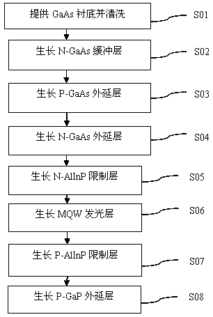
[0049] S1: Take a 2-inch N-type GaAs substrate with crystal orientation 0 >, the thickness is about 290um, using sulfuric acid: water: hydrogen peroxide = 3:1:1, at 45 ℃, carry out chemical cleaning in the mixed solution for 2Min, then wash away the deionized water, and then spin dry with nitrogen after 10Min.
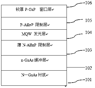
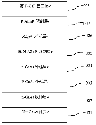
[0050] S2: Put the gallium arsenide substrate prepared in step S1 into the MOCVD epitaxial furnace, and grow an N-type GaAs buffer layer with a thickness of about 0.3-1.0um and a carrier concentration of about (1-8)×10 17 , the N-type GaAs buffer layer is used to achieve lattice matching with the GaAs substrate, and provides a fresh interface for the next growth; the N-type GaAs buffer layer is also a GaAlAs buffer layer.
[0051] S3: grow a P-type GaAs epitaxial layer on the N-type GaAs buffer layer, the thickness of which is in the range of 0.5-2um, and the carrier concentration range is (1-10)×10 17 . The P-type GaAs layer may also be a P-type GaAlAs layer or a com...
Embodiment 2
[0058] S1: Take a 2-inch high-resistance GaAs substrate with a crystal orientation of and a thickness of about 250um. Use sulfuric acid: water: hydrogen peroxide = 3:1:1, and conduct 2Min in the mixed solution at a temperature of 45°C. After chemical cleaning, rinse with deionized water for 10 minutes, and then spin dry with nitrogen gas for later use.
[0059] S2: Put the arsenized substrate prepared in step S1 into an MOCVD epitaxial furnace, grow an N-type GaAs buffer layer with a thickness of about 0.3-1.0um, and the N-type GaAs buffer layer is used to achieve lattice matching with the GaAs substrate , and provide a fresh interface for the next step of growth.
[0060] S3: grow a P-type GaAs epitaxial layer on the N-type GaAs buffer layer, the thickness of which is in the range of 0.5-2um, and the carrier concentration range is (1-10)×10 17 . The P-type GaAs epitaxial layer may also be a P-type GaAlAs layer or a composite structure of GaAlAs / GaAs.
[0061] S4: growing ...
Embodiment 3
[0067] S1: Take a 2-inch intrinsic type GaAs substrate, crystal orientation 0 >, the thickness is about 320um, using sulfuric acid: water: hydrogen peroxide = 3:1:1, at 45°C, carry out chemical cleaning in the mixed solution for 2Min, then wash away the deionized water for 10Min and then spin dry with nitrogen for later use.
[0068] S2: Put the arsenized substrate prepared in step S1 into an MOCVD epitaxial furnace to grow a GaAlAs buffer layer with a thickness of about 0.3-1.0um, and then grow an N-type GaAs buffer layer with a thickness of about 0.3-1.0um.
[0069] S3: grow a P-type GaAs epitaxial layer on the N-type GaAs buffer layer, the thickness of which is in the range of 0.5-2um, and the carrier concentration range is (1-10)×10 17 . The P-type GaAs layer may also be a P-type GaAlAs layer or a composite structure of GaAlAs / GaAs.
[0070] S4: growing an N-type GaAs epitaxial layer on the P-type GaAs epitaxial layer; the N-type GaAs epitaxial layer is also an N-type GaA...
PUM
| Property | Measurement | Unit |
|---|---|---|
| Thickness | aaaaa | aaaaa |
| Thickness | aaaaa | aaaaa |
| Thickness range | aaaaa | aaaaa |
Abstract
Description
Claims
Application Information