Micro light emitting element and manufacturing method thereof

A technology for light-emitting elements and manufacturing methods, which is applied to electrical elements, semiconductor devices, circuits, etc., and can solve the problems of production yield decline, N electrode detachment, etc.

Active Publication Date: 2018-09-18
TIANJIN SANAN OPTOELECTRONICS
View PDF4 Cites 5 Cited by
  • Summary
  • Abstract
  • Description
  • Claims
  • Application Information

AI Technical Summary

Problems solved by technology

However, when the wet etching process removes the substrate, the GaAs ohmic contact layer 111 is very thin and fragile (usually within 100nm). Yield drop

Method used


Image

  • Micro light emitting element and manufacturing method thereof
  • Micro light emitting element and manufacturing method thereof
  • Micro light emitting element and manufacturing method thereof

Examples


specific Embodiment

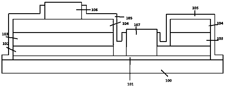
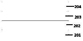
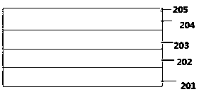
[0032] Concrete preparation method of the present invention is as follows:

[0033] (1) Provide LED epitaxy structure

[0034] like figure 2 As shown, an epitaxial structure is provided, which may generally include a growth substrate and an epitaxial stack thereon. The growth substrate 201 is selected from gallium arsenide, gallium arsenide, or gallium phosphide, etc., and its surface structure can be a planar structure or a patterned structure. The epitaxial stack includes a growth substrate 201, a GaAs buffer layer 202, (GaInP lattice transition layer is preferably provided), ohmic contact layer, window layer (buffer layer, ohmic contact layer, window layer are not shown in the figure), first semiconductor layer 202, active layer 203, second semiconductor layer 204, current spreading layer (not shown in the figure). The growth substrate 201 is used for epitaxial growth, and a suitable buffer layer material is set according to the growth substrate to eliminate the influen...


PUM

PropertyMeasurementUnit
thicknessaaaaaaaaaa
thicknessaaaaaaaaaa
thicknessaaaaaaaaaa

Abstract

The invention discloses a micro light emitting element and a manufacturing method thereof. By use of a temporary substrate, an epitaxial structure of a micro light emitting element made of a gallium arsenide and gallium phosphide substrate is transferred. After an epitaxial growing substrate is removed, the following preparation technology of the micro light emitting element is performed. Comparedwith the traditional technology where a chip structure is prepared by use of the epitaxial structure, corrosion to the epitaxial side face can be effectively avoided when the growing substrate is removed through wet etching.

Description

technical field [0001] The invention belongs to the field of semiconductor manufacturing, and in particular relates to a micro light-emitting element and a manufacturing method thereof. Background technique [0002] Micro light-emitting elements, that is (Micro LED, also known as μ-LED), in addition to OLED self-illumination, thin thickness, light weight, large viewing angle, short response time, high luminous efficiency, etc., it is easier to achieve high PPI (pixel density) , small size, easy to carry, low power consumption and other excellent characteristics, many units in the LED industry have devoted themselves to the development and application of components. Due to the small size of Micro LED, the structure is easily damaged during the manufacturing process, which affects the final product yield. As recorded in the patent technology CN201710763086.7, in the process of preparing Micro LED with the horizontal epitaxial structure of the existing gallium arsenide, galliu...

Claims


Application Information

Patent Timeline
Patent Type & Authority Applications(China)
IPC IPC(8): H01L33/00H01L33/36H01L33/48H01L33/52
CPCH01L33/30
Inventor 蔡景元钟秉宪吴俊毅
Owner TIANJIN SANAN OPTOELECTRONICS
Why Eureka
Try Eureka