A light-emitting diode epitaxial wafer and its manufacturing method

A technology of light-emitting diodes and manufacturing methods, which is applied to semiconductor devices, electrical components, circuits, etc., and can solve problems such as increased heat generation of LED chips and decreased LED light efficiency

Active Publication Date: 2020-07-07
HC SEMITEK ZHEJIANG CO LTD
View PDF8 Cites 0 Cited by
  • Summary
  • Abstract
  • Description
  • Claims
  • Application Information

AI Technical Summary

Problems solved by technology

[0005] Since the mobility of electrons is much higher than that of holes, electrons can quickly enter the multi-quantum well layer, and cross the multi-quantum well layer and undergo non-radiative recombination with holes in the P-type layer, which leads to an increase in the heat generation of the LED chip. Decreased light effect

Method used


Image

  • A light-emitting diode epitaxial wafer and its manufacturing method
  • A light-emitting diode epitaxial wafer and its manufacturing method
  • A light-emitting diode epitaxial wafer and its manufacturing method

Examples


Embodiment 1

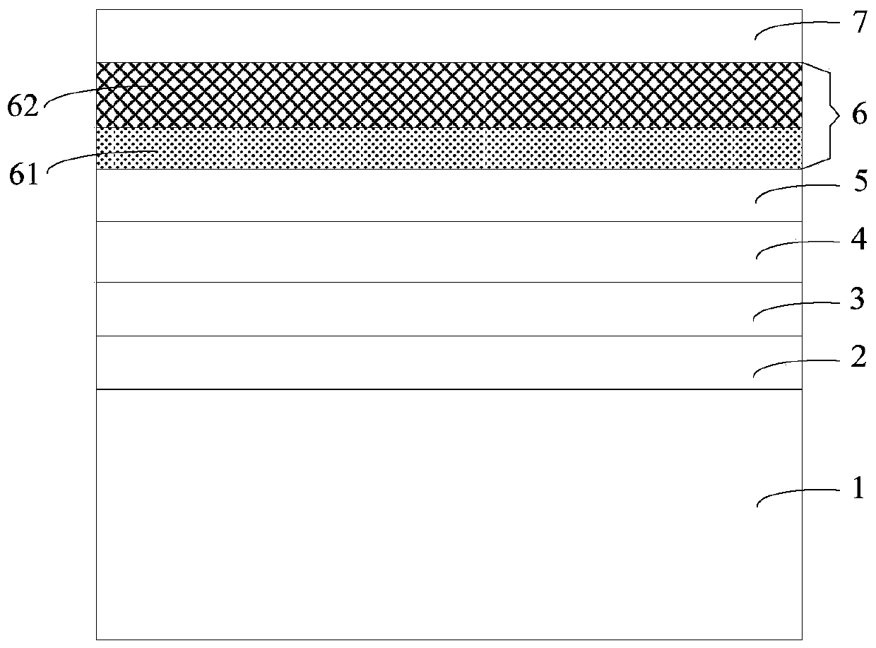
[0031] An embodiment of the present invention provides a light emitting diode epitaxial wafer, figure 1 It is a schematic structural diagram of a light-emitting diode epitaxial wafer provided by an embodiment of the present invention, as shown in figure 1 As shown, the light-emitting diode epitaxial wafer includes a substrate 1, a buffer layer 2, an undoped GaN layer 3, an N-type layer 4, a multi-quantum well layer 5, and a P-type doped layer 6 stacked on the substrate 1 in sequence. and P-type contact layer 7.

[0032] The P-type doped layer 6 includes at least one stacked structure, each stacked structure includes a first sub-layer 61 and a second sub-layer 62 that are sequentially stacked, and the first sub-layer 61 is Mg-doped Al x Ga 1-x N layer, 0y Ga 1-y N layers, 0

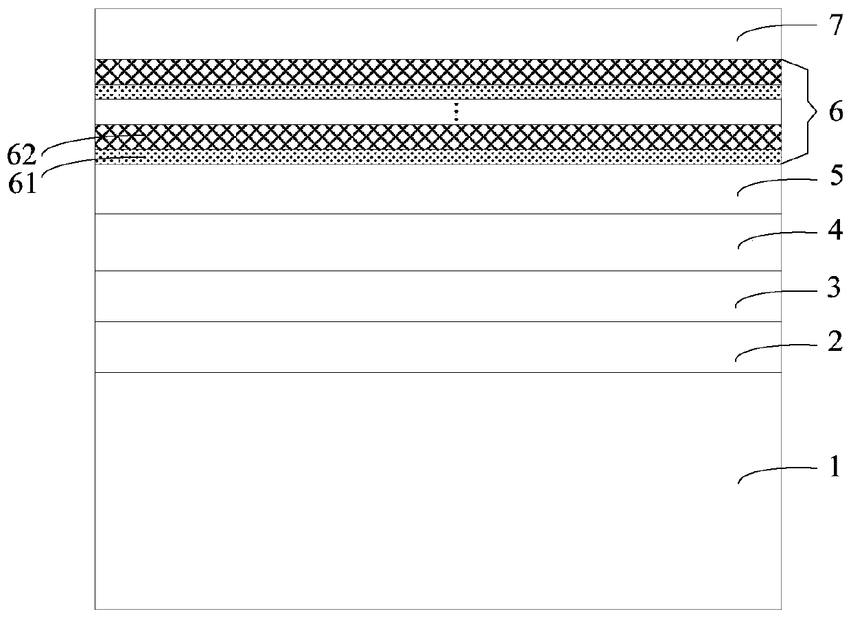
[0033] figure 1 The shown P-type doped layer 6 includes a laminated structure, figure 2 It is a schematic structural diagram of another light-emitting diode epitaxial wafer provided by the em...

Embodiment 2

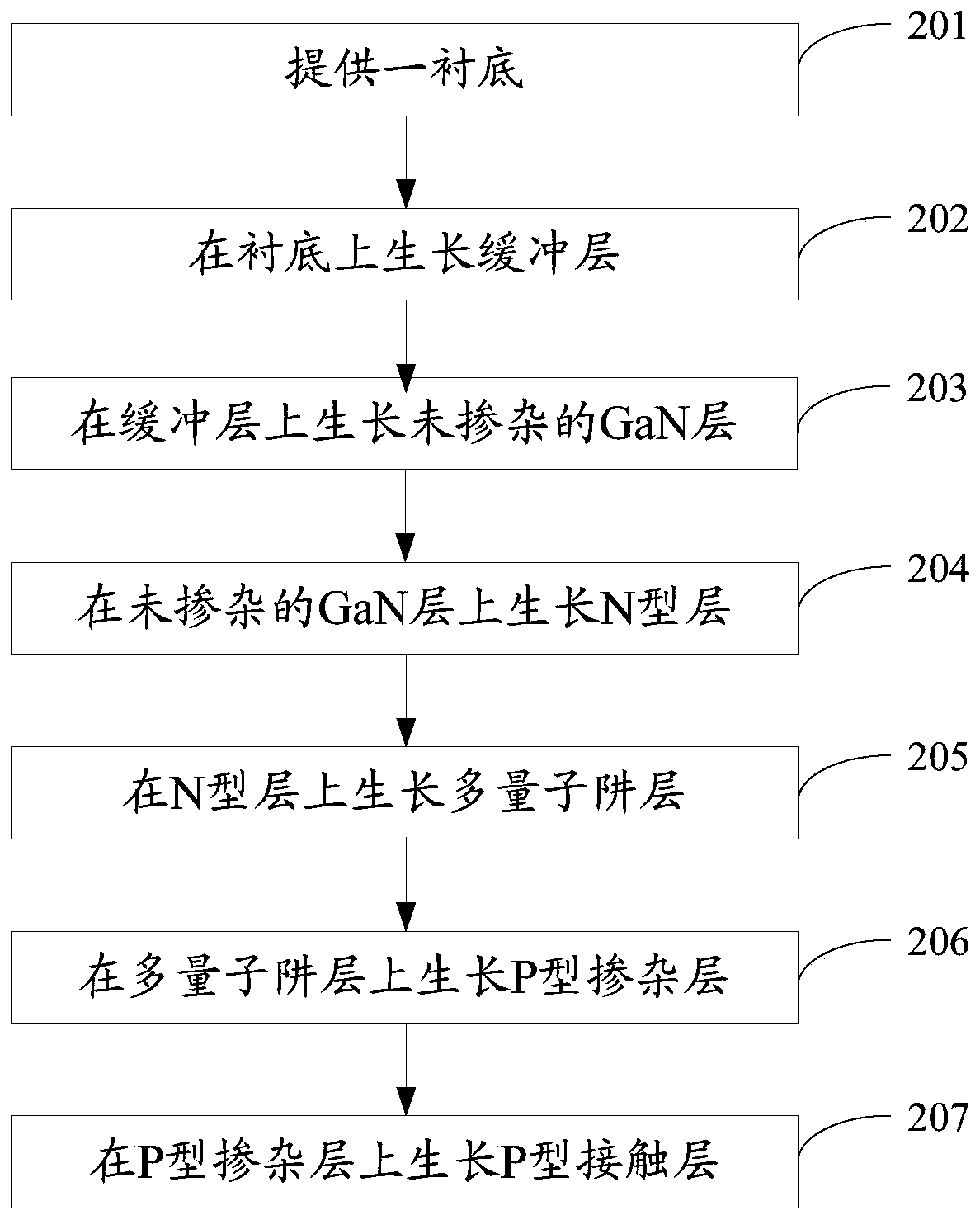
[0053] An embodiment of the present invention provides a method for manufacturing a light-emitting diode epitaxial wafer, which is used to manufacture the light-emitting diode epitaxial wafer provided in Embodiment 1, image 3 It is a method flowchart of a method for manufacturing a light-emitting diode epitaxial wafer provided by an embodiment of the present invention, as shown in image 3 As shown, the manufacturing method includes:

[0054] Step 201, providing a substrate.

[0055] Optionally, the substrate is sapphire.

[0056] In this embodiment, Veeco K465i or C4 MOCVD (Metal Organic Chemical Vapor Deposition, Metal Organic Compound Chemical Vapor Deposition) equipment can be used to realize the LED growth method. Using high-purity H 2 (hydrogen) or high-purity N 2 (nitrogen) or high purity H 2 and high purity N 2 The mixed gas as the carrier gas, high-purity NH 3 As the N source, trimethylgallium (TMGa) and triethylgallium (TEGa) are used as the gallium source, t...


PUM

PropertyMeasurementUnit
thicknessaaaaaaaaaa
thicknessaaaaaaaaaa
thicknessaaaaaaaaaa

Abstract

The invention discloses a light-emitting diode epitaxial wafer and a manufacturing method thereof, and belongs to the technical field of semiconductors. The light-emitting diode epitaxial wafer comprises a substrate, and a buffer layer, a non-doped GaN layer, an N-type layer, a multiple quantum well layer, a P-type doping layer and a P-type contact layer which are laminated on the substrate in sequence, wherein the P-type doping layer comprises at least one laminated structure; when the P-type doping layer comprises a plurality of laminated structures, the laminated structures are arranged ina laminated manner in sequence, each laminated structure comprises a first sub-layer and a second sub-layer which are arranged in the laminated manner in sequence, each first sub-layer is an Mg-dopedAlxGa1-xN layer, x is greater than 0 and smaller than or equal to 0.3, each second sub-layer is an Mg-doped InyGa1-yN layer, and y is greater than 0 and smaller than or equal to 0.2. The P-type dopinglayer can block electrons from moving towards a P-type layer, and simultaneously effective injection of holes is improved, so that the electrons and the holes give out light compositely through the radiation on the multiple quantum well layer, and then the lighting effect of an LED is improved.

Description

technical field [0001] The invention relates to the technical field of semiconductors, in particular to a light-emitting diode epitaxial wafer and a manufacturing method thereof. Background technique [0002] LED (Light Emitting Diode, Light Emitting Diode) is a semiconductor electronic component that can emit light. As an efficient, environmentally friendly and green new solid-state lighting source, it is being rapidly and widely used, such as traffic lights, car interior and exterior lights, urban landscape lighting, mobile phone backlights, etc. [0003] The epitaxial wafer is the main component of the LED. The existing GaN-based LED epitaxial wafer includes a substrate and a buffer layer stacked on the substrate in sequence, an undoped GaN layer, an N-type layer, a multi-quantum well layer, and a P-type layer. layer and the P-type contact layer. Among them, the N-type layer is doped with Si to provide electrons; the P-type layer is doped with Mg to provide holes; when ...

Claims


Application Information

Patent Timeline
Patent Type & Authority Patents(China)
IPC IPC(8): H01L33/24H01L33/06H01L33/00
CPCH01L33/005H01L33/06H01L33/24
Inventor 丁杰秦双娇胡任浩
Owner HC SEMITEK ZHEJIANG CO LTD
Why Eureka
Try Eureka