GaAs epitaxial film based on SOI substrate, preparation method and application
An epitaxial thin film and FD-SOI technology, which is applied in semiconductor/solid-state device manufacturing, electrical components, electrical solid-state devices, etc., to achieve the effects of reducing dislocation density, improving quality, and low energy consumption
- Summary
- Abstract
- Description
- Claims
- Application Information
AI Technical Summary
Problems solved by technology
Method used
Image

Examples
Embodiment 1
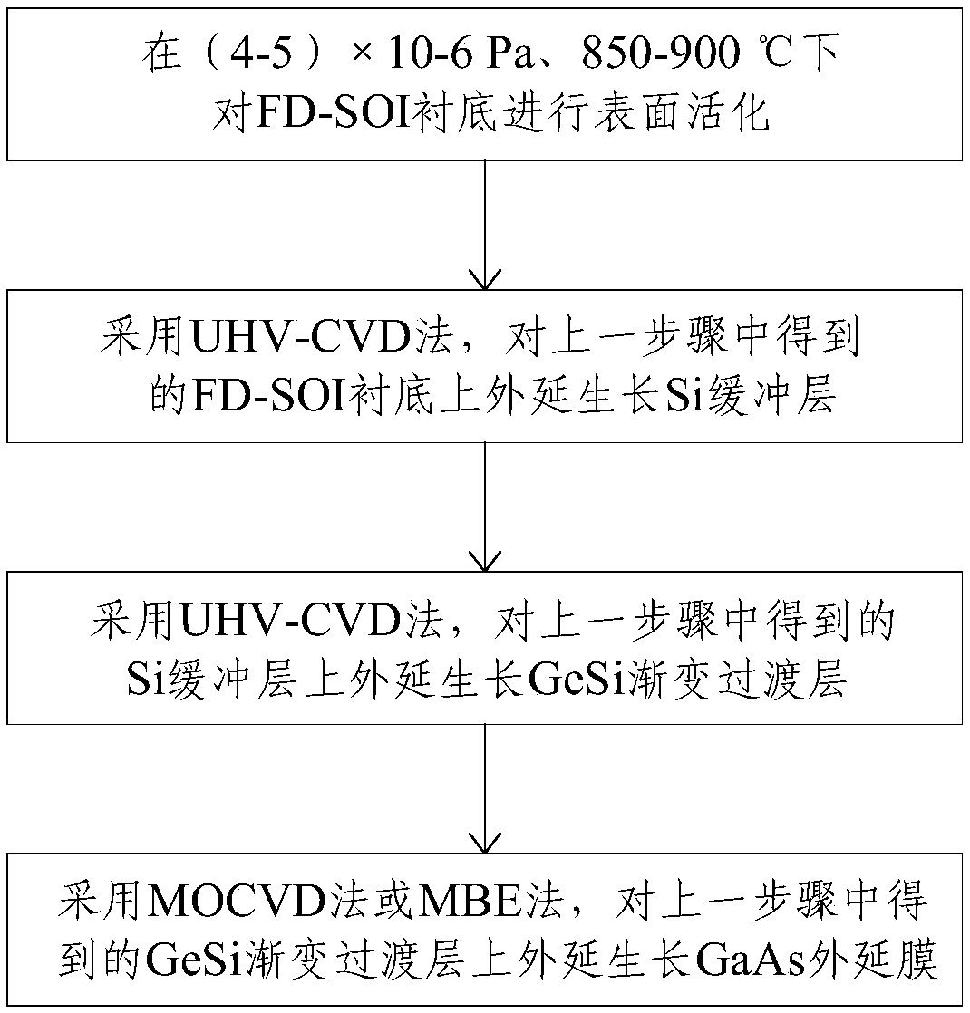
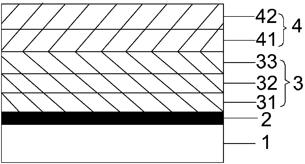
[0036] An embodiment of the present invention provides a method for preparing a GaAs epitaxial thin film based on an SOI substrate, comprising the following steps:
[0037] S1. Select the FD-SOI substrate for RCA cleaning and place it in the reaction chamber of the UHV-CVD system to maintain a vacuum of 5×10 - 6 Pa, slowly heat the substrate to 900°C and keep it for 30min for pretreatment;
[0038] S2. Lower the temperature of the substrate to 750°C and inject Si 2 h 6 Growth of 100nm Si buffer layer;
[0039] S3. Lower the temperature of the substrate to 450°C, and at the same time introduce the source material Si 2 h 6 and GeH 4 , start Ge x Si (1-x) Gradient transition layer growth: grow Ge first 0.24 Si 0.76 50min, then stop feeding Si 2 h 6 , lower the temperature to 330°C and continue to grow the low-temperature Ge layer for 2 hours. After the growth of the low-temperature Ge layer is completed, the temperature is adjusted to 600°C. After growing the high-pu...
Embodiment 2
[0042] An embodiment of the present invention provides a method for preparing a GaAs epitaxial thin film based on an SOI substrate, comprising the following steps:
[0043] S1. Select the FD-SOI substrate for RCA cleaning and place it in the reaction chamber of the UHV-CVD system to maintain a vacuum of 4×10 - 6 Pa, slowly heat the substrate to 850°C and keep it for 30min for pretreatment;
[0044] S2. Lower the temperature of the substrate to 750°C and inject Si 2 h 6 Growth of 100nm Si buffer layer;
[0045] S3, using SiH based on UHV-CVD 4 / Si 2 h 6 , GeH 4 As a growth source, the gas pressure is 30mTorr, using Ge x Si (1-x) Gradual buffering of medium Ge composition, low dislocation density and good crystal quality Ge grown at a temperature of 400°C x Si (1-x) Gradient transition layer: first grow the first layer of Si with a thickness of 0.8 μm 0.1 Ge 0.9 , and by in-situ annealing at 660 °C for 15 min; subsequently growing a second layer of Si with a thickne...
Embodiment 3
[0048] An embodiment of the present invention provides a method for preparing a GaAs epitaxial thin film based on an SOI substrate, comprising the following steps:
[0049] S1. Select the FD-SOI substrate for RCA cleaning and place it in the reaction chamber of the UHV-CVD system to maintain a vacuum of 5×10 - 6 Pa, slowly heat the substrate to 900°C and keep it for 30min for pretreatment;
[0050] S2. Lower the temperature of the substrate to 750°C and inject Si 2 h 6 Growth of 100nm Si buffer layer;
[0051] S3. Lower the temperature of the substrate to 450°C, and at the same time introduce the source material Si 2 h 6 and GeH 4 , start Ge x Si (1-x) Gradient transition layer growth: grow Ge first 0.24 Si 0.76 50min, then stop feeding Si 2 h 6 , lower the temperature to 330°C and continue to grow the low-temperature Ge layer for 2 hours. After the growth of the low-temperature Ge layer is completed, the temperature is adjusted to 600°C. After growing the high-pu...
PUM
 Abstract
Description
Claims
Application Information
 - R&D
- Intellectual Property
- Life Sciences
- Materials
- Tech Scout
- Unparalleled Data Quality
- Higher Quality Content
- 60% Fewer Hallucinations
Browse by: Latest US Patents, China's latest patents, Technical Efficacy Thesaurus, Application Domain, Technology Topic, Popular Technical Reports.
© 2025 PatSnap. All rights reserved.Legal|Privacy policy|Modern Slavery Act Transparency Statement|Sitemap|About US| Contact US: help@patsnap.com