High thermal conductivity package substrate and preparation method thereof

A packaging substrate, high thermal conductivity technology, applied in the direction of circuit heating devices, printed circuit components, etc., can solve the problems of laser drilling technology, complex preparation process, complex heat conduction path, etc., to achieve stable size, simple manufacturing process, and heat conduction simple path effect

Pending Publication Date: 2018-09-25
NINGBO HUAYUAN ELECTRONICS TECH
View PDF4 Cites 3 Cited by
  • Summary
  • Abstract
  • Description
  • Claims
  • Application Information

AI Technical Summary

Problems solved by technology

[0004] At present, packaging substrates with high thermal conductivity and high insulation are generally divided into three types: 1. Through-hole conduction FPC board + ceramic board. The heat conduction path of this structure is: ceramic board→tin foil→IMC layer→tin+soft board hole copper→conduction Glue → steel sheet, the advantage is that the circuit board process is relatively simple, but the disadvantages are: it must be matched with a ceramic substrate, the heat conduction path is complicated, the heat conduction area is small, the heat dissipation is average, and the tin in the via hole cannot be completely filled
2. Blind holes conduct FPC board + ceramic board. The heat conduction path of this structure is: ceramic board→tin foil→IMC layer→tin+soft board hole copper→conductive glue→steel sheet. The advantage is: the circuit board process is relatively simple. , no risk of solder voids, the disadvantages are: it must be matched with a ceramic substrate, the heat conduction path is complicated, the heat conduction area is small, the heat dissipation is not good, and there is a laser drilling process
3. High thermal conductivity soft and hard combination package substrate. The heat conduction path of this structure is: ceramic plate pad→copper pillar→pure copper reinforcement plate. Its advantages are: good heat dissipation, the heat dissipation medium is pure copper, and there is no need to use ceramic substrate , the total plate thickness is adjustable, the disadvantage is: the cost increases
This packaging substrate uses micro heat pipes and high thermal conductivity ceramic circuit boards to achieve metallurgical bonding through vacuum welding, vacuum friction welding, active metal brazing, nano-silver welding, etc., to reduce thermal resistance and achieve efficient heat dissipation, but the preparation process is also relatively complicated. The cost is also higher

Method used


Image

  • High thermal conductivity package substrate and preparation method thereof
  • High thermal conductivity package substrate and preparation method thereof
  • High thermal conductivity package substrate and preparation method thereof

Examples


Embodiment Construction

[0044] The present invention will be further described in detail below in conjunction with the accompanying drawings and embodiments.

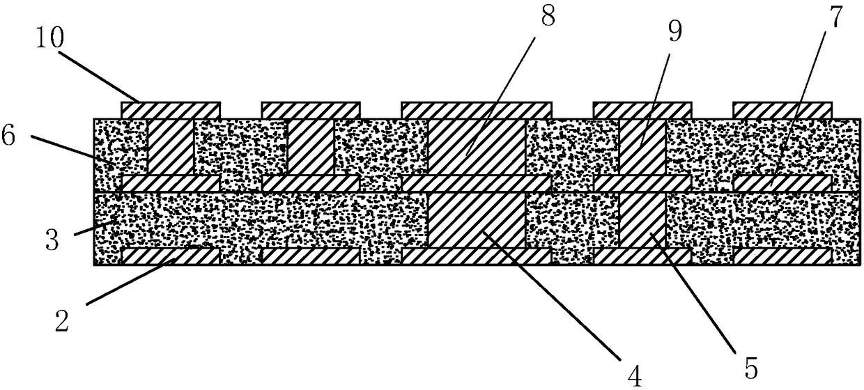
[0045] Such as Figure 1-10 As shown, a high thermal conductivity packaging substrate, the high thermal conductivity packaging substrate includes:

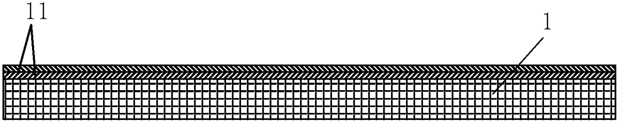
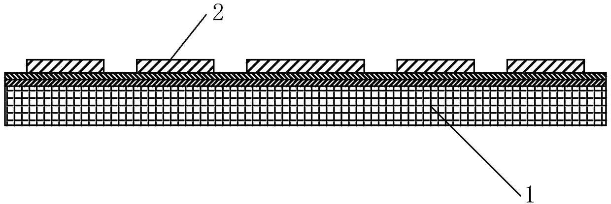
[0046] A copper substrate 1, the upper surface of the copper substrate 1 is plated with a metal protective layer 11;

[0047] The first layer of wiring 2 is additively plated on the upper surface of the copper substrate 1, and the first layer of wiring 2 is additively plated with a first conduction copper column 5 and a first heat dissipation copper column 4;

[0048] The first insulating layer 3 is pressed on the upper surface of the metal protection layer 11 of the copper substrate 1 and covers the first layer of wiring 2;

[0049] The second layer of wiring 7 is additively plated on the upper surface of the first insulating layer 3, and correspondingly, the second layer of wiring 7 is additiv...


PUM

PropertyMeasurementUnit
diameteraaaaaaaaaa
diameteraaaaaaaaaa
diameteraaaaaaaaaa

Abstract

A high thermal conductivity package substrate and a preparation method thereof are disclosed. The preparation method includes the steps of: electroplating a copper substrate with a metal protective layer; addition-electroplating the copper substrate with a first line layer; forming a first conductive copper post and a first heat-dissipating copper post on the first line layer, and electroplating the first conductive copper post and the first heat-dissipating copper post; pressing a first insulating layer on the first line layer and performing grinding; forming a second line layer on the firstinsulating layer; forming a second conductive copper post and a second heat dissipating copper post on the second line layer, and pressing a second insulating layer on the second line layer and performing grinding; forming a third line layer on the second insulating layer; and etching the copper substrate. The heat-dissipating copper posts can allow a simple heat conductive path, and the heat dissipating effect is improved; the preparation process is simple, the cost is low, the prepared high thermal conductivity package substrate is stable in size, the conductive path is simple, and the heatdissipating performance is excellent.

Description

technical field [0001] The invention relates to the technical field of printed circuit board manufacturing, in particular to a high thermal conductivity packaging substrate and a preparation method thereof. Background technique [0002] Packaging substrates are often used in the field of semiconductor packaging technology, and the packaging substrate is Substrate (SUB for short), which is a term in printed circuit boards. The substrate can provide the chip with electrical connection, protection, support, heat dissipation, assembly and other functions to achieve multi-pin, reduce the volume of packaged products, improve electrical performance and heat dissipation, ultra-high density or multi-chip modularization. At present, packaging substrates are developing in the direction of high density. [0003] Packaging technology is critical to the functionality of power semiconductor devices. Good electrical isolation and thermal management, minimum parasitic capacitance, and very...

Claims


Application Information

Patent Timeline
Patent Type & Authority Applications(China)
IPC IPC(8): H05K1/02
CPCH05K1/0203
Inventor 张成立徐光龙王强
Owner NINGBO HUAYUAN ELECTRONICS TECH
Why Eureka
Try Eureka