
Device with storage and gating functions and preparation method thereof

A dual-function, device technology, applied in electrical components and other directions, can solve problems such as low device density

Active Publication Date: 2018-09-28
HUBEI UNIV
View PDF6 Cites 1 Cited by
  • Summary
  • Abstract
  • Description
  • Claims
  • Application Information

AI Technical Summary

Problems solved by technology

But this solution needs to connect two kinds of components in series, and the device density is small

Method used


Image

  • Device with storage and gating functions and preparation method thereof
  • Device with storage and gating functions and preparation method thereof
  • Device with storage and gating functions and preparation method thereof

Examples


preparation example Construction

[0031] The present invention also provides a method for preparing the storage and gating dual-function device described in the above technical solution, comprising the following steps:

[0032] (1) Using argon as the working gas and niobium pentoxide target as the sputtering target, perform the first sputtering on the surface of the bottom electrode to obtain the semi-finished product of the storage and gating dual-function device;

[0033] (2) Using argon as the working gas and a tungsten target as the sputtering target, perform the second sputtering on the niobium oxide surface of the semi-finished storage and gating dual function device to obtain the storage and gating dual function device.

[0034] In the present invention, a tungsten target and a niobium pentoxide target are preferably installed on the magnetron sputtering equipment, and then after the vacuum chamber of the magnetron sputtering equipment is evacuated, argon gas is introduced to the pressure required for th...

Embodiment 1

[0051] (1) will have an area of ​​1μm 2 The surface of the base material of the TiN bottom electrode is rinsed with high-pressure air for subsequent use; the TiN bottom electrode is square and has a thickness of 200nm;

[0052] (2) Install a tungsten target and a niobium pentoxide target in the magnetron sputtering equipment, place the mold carrier substrate with the TiN bottom electrode obtained in step (1) in the magnetron sputtering equipment, and place the vacuum chamber After evacuating, argon is introduced until the system pressure is 4 Torr;

[0053] (3) Turn on the radio frequency measurement and control sputtering power supply, and at a temperature of 300K, with a power of 120W, sputter niobium pentoxide to the surface of the TiN bottom electrode for 400s, then turn off the radio frequency magnetron sputtering to obtain a semi-finished product;

[0054] (4) Turn on the DC magnetron sputtering power supply, and sputter tungsten on the surface of the semi-finished produc...


PUM

PropertyMeasurementUnit
thicknessaaaaaaaaaa
thicknessaaaaaaaaaa
areaaaaaaaaaaa

Abstract

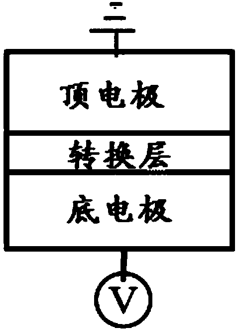
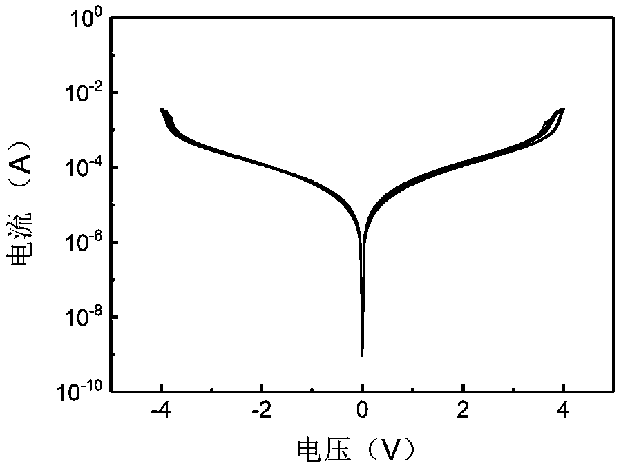
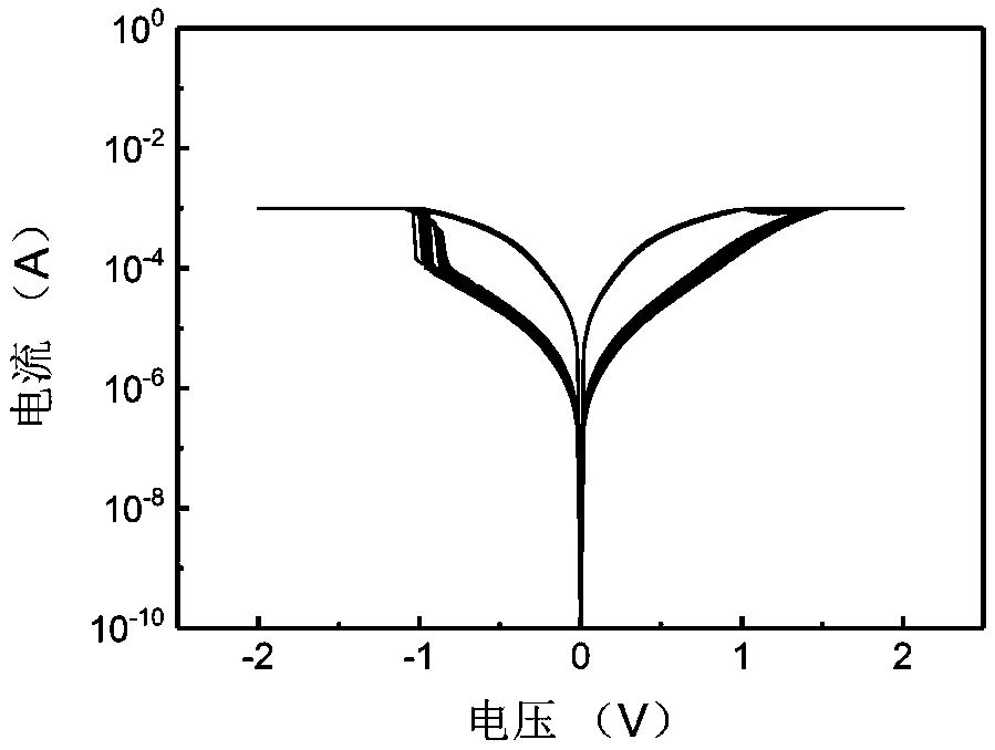
The invention provides a device with storage and gating functions which comprises a bottom electrode, a conversion layer and a top electrode sequentially from downside to upside; the bottom electrodeis TiN or conductive glass; the conversion layer is made of niobium oxide; and the top electrode is tungsten. The device with the storage and gating functions is composed of the niobium oxide which serves as the conversion layer, the TiN or conductive glass which serves as the bottom electrode, and the metal tungsten which serves as the top electrode. The experimental results show that the deviceprovided by the invention has a gating function in the presence of big current limitation and has a resistance change performance (storage performance) in the presence of small current limitation; thedevice also has excellent stability as the deviation degree of the obtained curve is very small after the device is subjected to circular test for 100 turns in the gating and resistance change performance test; and the device also has a relatively big storage window as the resistance value of a high-resistance resistor is 10 greater than that of a low-resistance resistor in the resistance changeperformance test.

Description

technical field [0001] The invention relates to the technical field of electronic materials and components, in particular to a storage and gating dual-function device and a preparation method thereof. Background technique [0002] Traditional charge-based memories, such as NAND flash memory, face physical and technical limitations of scalability, which has become a bottleneck for their development. Resistive Random Access Memory (RRAM) is considered as one of the candidates for the next generation of Non-Volatile Memory (NVM). RRAM has the advantages of simple device structure, excellent scalability, fast switching speed, potential 3D memory architecture, excellent data retention and compatibility with complementary metal-oxide-semiconductor (CMOS) technology. To achieve high-density memory, RRAM is envisioned for 3D interleaved array memory cells, however, one of the main drawbacks of this structure is the problem of sneak paths through adjacent memory cells. This issue c...

Claims


Application Information

Patent Timeline
Patent Type & Authority Applications(China)
IPC IPC(8): H01L45/00
CPCH10N70/20H10N70/841H10N70/883H10N70/011
Inventor 王浩何玉立陈傲马国坤陈钦
Owner HUBEI UNIV
Learn More