Anti-PID (Potential Induced Degradation) assembly and manufacturing method thereof

A technology for components and lamination equipment, applied in electrical components, semiconductor devices, photovoltaic power generation, etc., can solve the problems of increasing silicon nitride thickness, square resistance fluctuation, increasing component cost, etc., and achieve good conductivity and high transmittance. , strong adsorption effect

Inactive Publication Date: 2018-10-02
TAIZHOU ZHONGLAI PHOTOELECTRIC TECH CO LTD
View PDF4 Cites 4 Cited by
  • Summary
  • Abstract
  • Description
  • Claims
  • Application Information

AI Technical Summary

Problems solved by technology

However, these materials tend to be significantly more expensive than more PID-prone competing materials such as EVA
Second, research has demonstrated that anti-reflective, passivating coatings applied to the PV cells themselves can have significant effects, which has resulted in the design of protective cell coatings that can reduce PID effects using methods that sometimes include increasing density and / or thickness , such as methods for non-porous silicon nitride cell coatings, a complication of silicon nitride modification is that it also sub-optimizes the refractive index or complicates process control and cost, increasing silicon nitride thickness increases cost and also Lower overall module conversion efficiency
However, in this method, it is difficult for nanoparticles to be uniformly dispersed in the sol, resulting in large fluctuations in square resistance.
In addition, in order to obtain a lower square resistance, a large number of nanoparticles and nano-conductive materials must be used, which will inevitably increase the cost of the component and affect the optical properties of the component

Method used


Image

  • Anti-PID (Potential Induced Degradation) assembly and manufacturing method thereof

Examples


Embodiment Construction

[0050] The present invention will be described in detail below in conjunction with the embodiments. It should be noted that the described embodiments are only intended to facilitate the understanding of the present invention, and have no limiting effect on it.

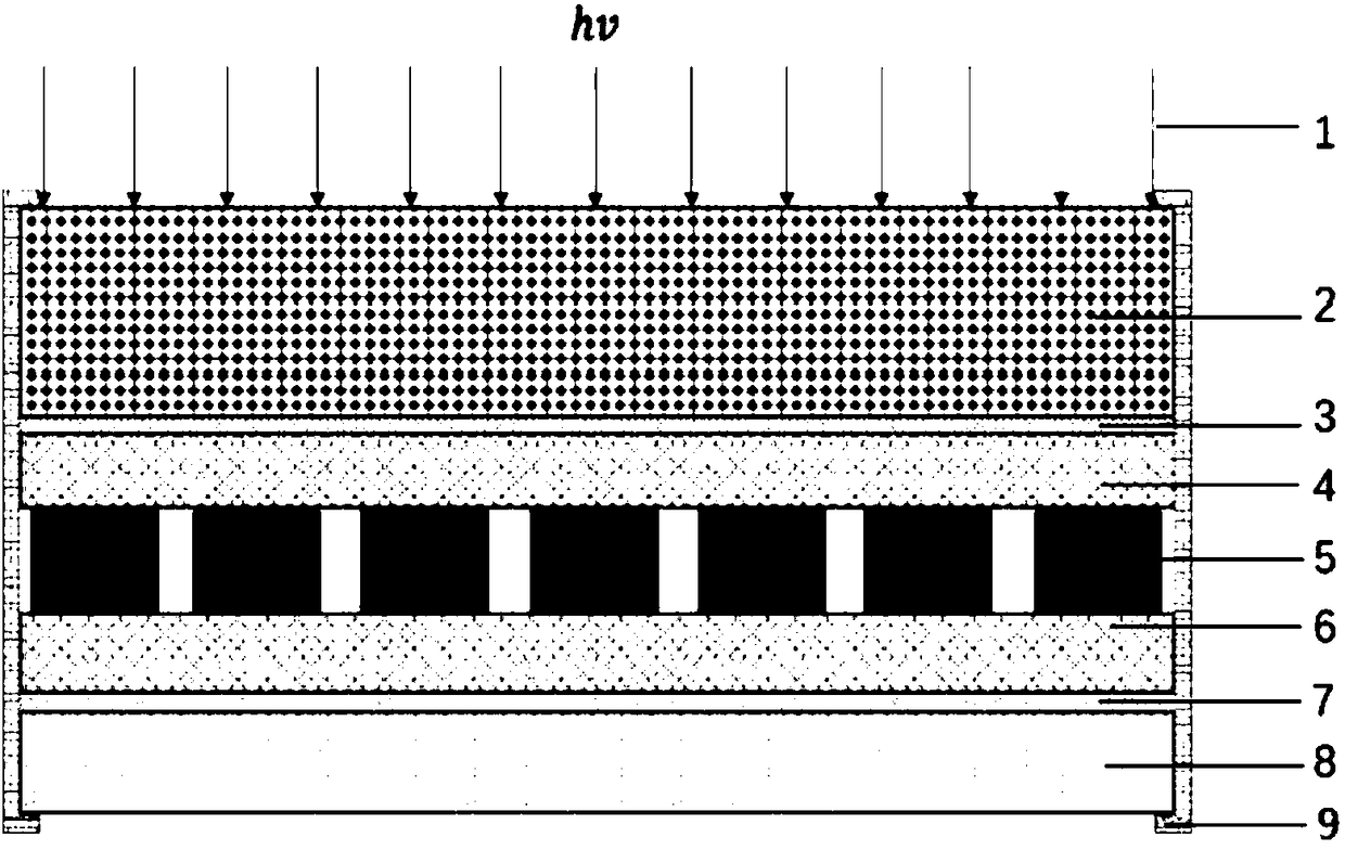
[0051] According to an anti-PID assembly provided by the present invention, it includes a front glass 2, a first encapsulation layer 4, at least one photovoltaic solar cell 5, a second encapsulation layer 6, a back plate 8 and an assembly frame 9, the front glass 2 and the first encapsulation layer An ultra-thin two-dimensional electrical nanomaterial layer is arranged between the first encapsulation layer 4 and between the second encapsulation layer 6 and the backplane 8;

[0052] The side of the ultra-thin two-dimensional electrical nanomaterial layer is connected to the frame 9 of the component.

[0053] Among them, preferably, both the first encapsulation layer 4 and the second encapsulation layer 6 are cut EVA.

...


PUM


Abstract

The invention relates to an anti-PID (Potential Induced Degradation) assembly and a manufacturing method thereof. The anti-PID assembly comprises front panel glass, a first packaging layer, at least one photovoltaic solar cell, a second packaging layer, a backplane and an assembly frame, wherein ultrathin two-dimensional electrical nano material layers are arranged between the front panel glass and the first packaging layer and between the second packaging layer and the backplane; and the side edges of the ultrathin two-dimensional electrical nano material layers are connected with the assembly frame. The ultrathin two-dimensional electrical nano material layer is adopted as an insertion layer of a solar module, the layer has strong absorbability, good conductivity and high transmittance and can thus play a good role of adsorbing ions, the ions are transferred to the assembly frame, and thus, accumulation of charges on the surface of the cell caused by ion migration to generate PID effects can be avoided; and due to the high transmittance, application of the two-dimensional nano material can be ensured not to affect the performance of the solar module.

Description

technical field [0001] The invention relates to the field of photovoltaic solar cells, in particular to an anti-PID component and a preparation method thereof. Background technique [0002] In recent years, with the continuous consumption of fossil energy and gradually becoming exhausted, solar energy, as a green renewable energy, is gradually entering people's lives. However, in recent years, the quality problems of power plants at home and abroad have appeared on a large scale, and many power plants have experienced quality problems such as Potential Induced Degradation (PID), which has led to a decline of up to 60% in the power plant after about one year of operation. [0003] PID means that the components work at high voltage for a long time, and there is leakage current between the cover glass, packaging material, and frame, which causes a large amount of charge to accumulate on the surface of the cell, deteriorating the passivation effect of the cell surface, resulting...

Claims


Application Information

Patent Timeline
Patent Type & Authority Applications(China)
IPC IPC(8): H01L31/0216H01L31/048
CPCY02E10/50H01L31/02167H01L31/0481
Inventor 王建明刘宗涛刘志锋
Owner TAIZHOU ZHONGLAI PHOTOELECTRIC TECH CO LTD
Why Eureka
Try Eureka