Organic light emitting diode containing multi-level organic semiconductor heterojunction

A technology for organic semiconductors and light-emitting diodes, which is applied in the fields of semiconductor devices, semiconductor/solid-state device manufacturing, electric solid-state devices, etc., which can solve the problems of commercialization and popularization of the preparation of high-performance organic light-emitting diodes, the distance from application is too large, and the crystallization conditions are harsh. and other problems, to achieve the effect of simplifying the structure and preparation process, efficient hole and electron transport characteristics, and good uniformity

Active Publication Date: 2018-10-16
SOUTH CHINA UNIV OF TECH
View PDF9 Cites 5 Cited by
  • Summary
  • Abstract
  • Description
  • Claims
  • Application Information

AI Technical Summary

Problems solved by technology

Although this can avoid problems such as the quenching effect caused by the introduction of dopants and the decrease in device stability, the implementation method is very difficult.
First of all, the crystallization conditions of these organic semiconductor materials are very harsh, and the crystallization time is long, which is a great challenge to the device preparation process
In addition, there are very few types of materials that can be crystallized, and there is still a long way to go before the application. Therefore, this method is still not conducive to the preparation and commercialization of high-performance organic light-emitting diodes.

Method used


Image

  • Organic light emitting diode containing multi-level organic semiconductor heterojunction
  • Organic light emitting diode containing multi-level organic semiconductor heterojunction
  • Organic light emitting diode containing multi-level organic semiconductor heterojunction

Examples


Embodiment 1

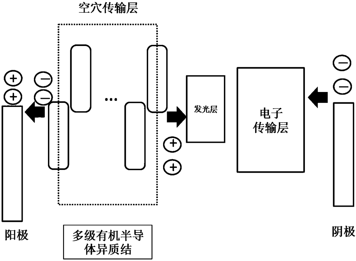
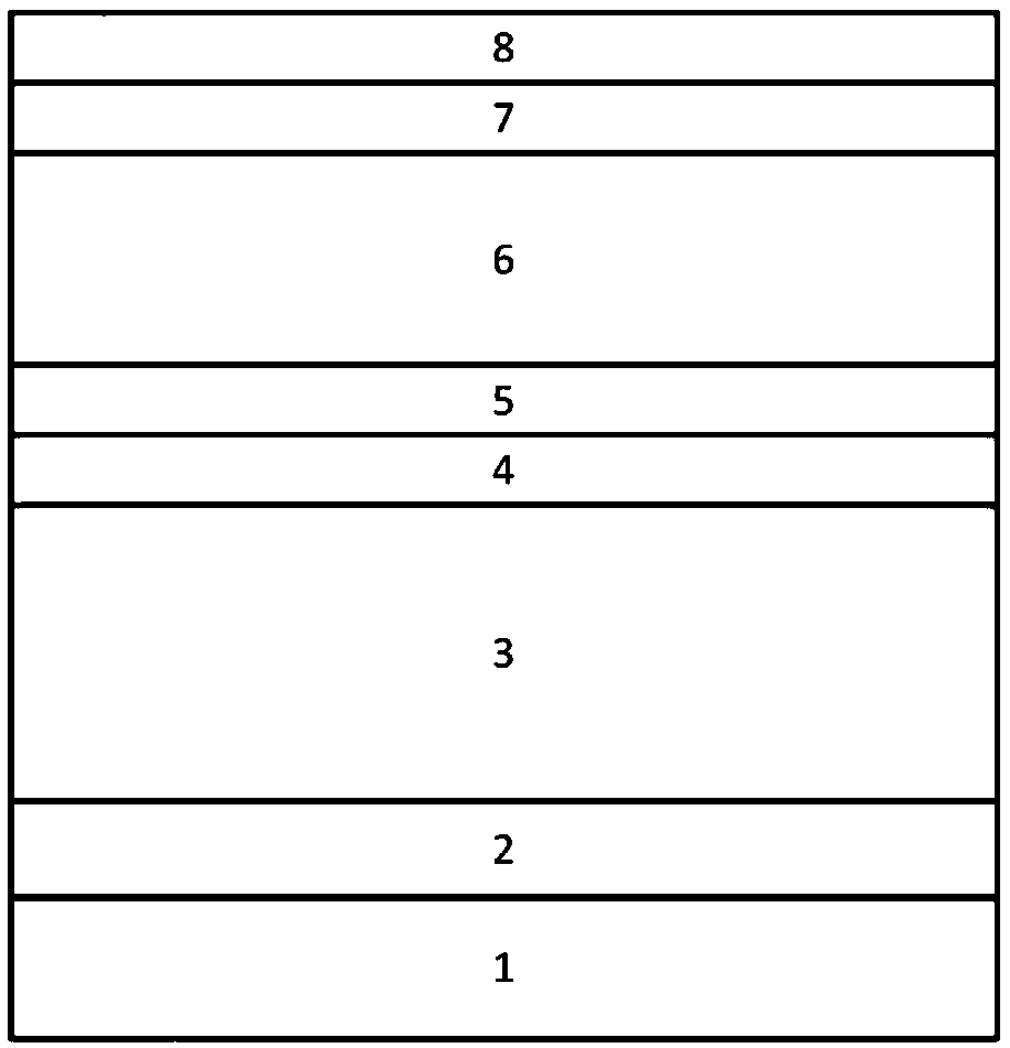
[0039] An organic light-emitting diode device using a multi-level organic semiconductor heterojunction as a hole transport layer in this embodiment, the schematic diagram of its working principle is as follows figure 1 As shown, the schematic diagram of its stacked structure is shown in figure 2 As shown, the substrate 1, anode 2, multi-level organic semiconductor heterojunction hole transport layer 3, light emitting layer 4, hole / exciton blocking layer 5, electron transport layer 6, electron injection layer 7 and Cathode 8 composition. It is prepared by the following method:

[0040] First, the ITO layer 2 of the substrate glass layer 1 is photolithographically formed into thin strip electrodes, then cleaned with lotion and rinsed with a large amount of deionized water, blown dry with nitrogen, and baked in a blast oven at 120 degrees for 20 minute. After drying, after 15 minutes of ultraviolet ozone treatment, it is directly transferred to the vacuum coating system until...

Embodiment 2

[0043] In this embodiment, an organic light-emitting diode device using a multi-level organic semiconductor heterojunction as a hole transport layer and an electron transport layer at the same time, the schematic diagram of its working principle is as follows Figure 8 As shown, the schematic diagram of its stacked structure is shown in Figure 9 As shown, the substrate 1, the anode 2, the multi-level organic semiconductor heterojunction hole transport layer 3, the light-emitting layer 4, the hole / exciton blocking layer 5, the electron injection layer 6, the multi-level organic semiconductor heterojunction stacked in sequence The mass junction electron transport layer 7 and the cathode 8 are composed. It is prepared by the following method:

[0044] First, the ITO layer 2 of the substrate glass layer 1 is photolithographically formed into thin strip electrodes, then cleaned with lotion and rinsed with a large amount of deionized water, blown dry with nitrogen, and baked in a ...

Embodiment 3

[0047] In this embodiment, an organic light-emitting diode device using a multi-level organic semiconductor heterojunction as a hole transport layer, an electron transport layer, and a charge generation layer at the same time, the schematic diagram of its working principle is as follows Figure 15 As shown, the schematic diagram of its stacked structure is shown in Figure 16 As shown, the substrate 1, the anode 2, the multi-level organic semiconductor heterojunction hole transport layer 3, the light-emitting layer 4, the hole / exciton blocking layer 5, the electron injection layer 6, the multi-level organic semiconductor heterojunction stacked in sequence It consists of a mass junction charge generation layer 7 , a light emitting layer 8 , a hole / exciton blocking layer 9 , an electron injection layer 10 , a multilevel organic semiconductor heterojunction electron transport layer 11 and a cathode 12 . It is prepared by the following method:

[0048] First, the ITO layer 2 of t...


PUM


Abstract

The invention belongs to the field of organic light emitting diodes, and discloses an organic light emitting diode containing a multi-level organic semiconductor heterojunction. At least one of a holetransport layer, an electron transport layer, and a charge generation layer in the organic light emitting diode containing the multi-level organic semiconductor heterojunction is formed by a multi-level organic semiconductor heterostructure, wherein the multi-level organic semiconductor heterojunction is formed by a p-type semiconductor material layer and an n-type semiconductor material layer inan alternate manner, wherein the number of layers of the p-type semiconductor material layer and the number of layers of the n-type semiconductor material layer are equal to 2 or greater. The organiclight emitting diode containing the multi-level organic semiconductor heterojunction of the invention employs the multi-stage organic semiconductor heterojunction structure, and has properties of efficient hole transport, electron transport and charge generation. The properties of efficient hole and electron transport allow it to completely replace conventional p-doped hole transport and n-dopedelectron transport.

Description

technical field [0001] The invention belongs to the field of organic light-emitting diodes, and in particular relates to an organic light-emitting diode containing multilevel organic semiconductor heterojunctions. Background technique [0002] Organic Light-emitting Diode OLED (Organic Light-emitting Diode OLED) has significant advantages such as high efficiency, fast response, wide color gamut, flexibility, thinness, planar light emission, energy saving and environmental protection, and has become the most promising lighting and flat panel display technology of the new generation. Organic light-emitting diodes have shown amazing effects whether they are used as the display screens of smart watches, mobile phones, TVs, or ordinary lighting fixtures. [0003] After years of research and development, the structure of organic light-emitting diodes has been perfected. High-efficiency organic light-emitting diodes usually use a sandwich structure in which an organic electrolumine...

Claims


Application Information

Patent Timeline
Patent Type & Authority Applications(China)
IPC IPC(8): H01L51/50H01L51/52
CPCH10K50/156H10K50/166H10K50/19
Inventor 马东阁代岩峰郭庆勋孙倩陈江山
Owner SOUTH CHINA UNIV OF TECH
Why Eureka
Try Eureka