A nitrogen dioxide sensor based on an organic thin film transistor and its preparation method

A technology of nitrogen dioxide and organic thin film, which is applied in the field of nitrogen dioxide sensor and its preparation, can solve the problems of low carrier mobility, poor crystallinity of film formation, etc., achieve high sensitivity and high response detection, improve surface roughness, Guaranteed effect of sensing performance

Active Publication Date: 2022-04-15
UNIV OF ELECTRONICS SCI & TECH OF CHINA
View PDF0 Cites 0 Cited by
  • Summary
  • Abstract
  • Description
  • Claims
  • Application Information

AI Technical Summary

Problems solved by technology

[0005] Aiming at the disadvantages of poor film-forming crystallinity and low carrier mobility in the above existing organic thin film transistor nitrogen dioxide sensors, the present invention provides a nitrogen dioxide sensor based on organic thin film transistors and a preparation method thereof

Method used


Image

  • A nitrogen dioxide sensor based on an organic thin film transistor and its preparation method
  • A nitrogen dioxide sensor based on an organic thin film transistor and its preparation method

Examples


Embodiment 1

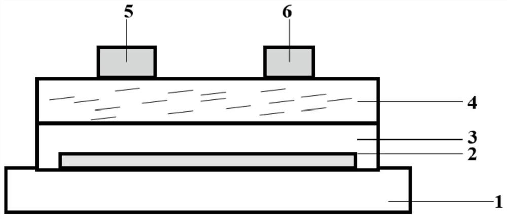
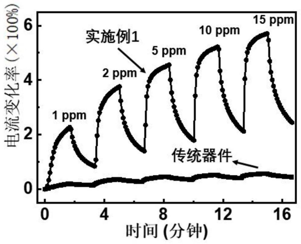
[0043] Such as Figure 1-2 As shown, a nitrogen dioxide sensor based on an organic thin film transistor, the nitrogen dioxide sensor includes a substrate 1, a gate electrode 2, a dielectric layer 3, an organic semiconductor layer 4, a source electrode 5 and a drain electrode in order from bottom to top 6. The organic semiconductor layer 4 is a mixed material of gold nanorods and organic semiconductor materials; wherein, the gate electrode 2, the source electrode 5 and the drain electrode 6 are all silver nanowires, and the dielectric layer 3 is made of polystyrene (PS) , the thickness is 500nm, the semiconductor layer 4 is formed by mixing P3HT and gold nanorod solution (concentration is 0.1mg / ml), and the thickness is 50nm. An organic thin film transistor nitrogen dioxide sensor with high sensitivity and high stability can be realized by using the structure. An organic thin film transistor nitrogen dioxide sensor with high sensitivity and high stability can be realized by us...

Embodiment 2

[0052] Such as figure 1 As shown, a nitrogen dioxide sensor based on an organic thin film transistor, the nitrogen dioxide sensor includes a substrate 1, a gate electrode 2, a dielectric layer 3, an organic semiconductor layer 4, a source electrode 5 and a drain electrode in order from bottom to top 6. The organic semiconductor layer 4 is a mixed material of gold nanorods and organic semiconductor materials; wherein, the gate electrode 2, the source electrode 5 and the drain electrode 6 are all gold nanowires, and the dielectric layer 3 is made of polymethyl methacrylate (PMMA), with a thickness of 300nm, and the semiconductor layer 4 is formed by mixing P3HT and gold nanorod solution (concentration: 0.3mg / ml), with a thickness of 70nm. An organic thin film transistor nitrogen dioxide sensor with high sensitivity and high stability can be realized by using the structure.

[0053] A method for preparing a nitrogen dioxide sensor based on an organic thin film transistor, compri...

Embodiment 3

[0060] Such as figure 1 As shown, a nitrogen dioxide sensor based on an organic thin film transistor, the nitrogen dioxide sensor includes a substrate 1, a gate electrode 2, a dielectric layer 3, an organic semiconductor layer 4, a source electrode 5 and a drain electrode in order from bottom to top 6. The organic semiconductor layer 4 is a mixed material of gold nanorods and organic semiconductor materials; wherein, the gate electrode 2, the source electrode 5 and the drain electrode 6 are all indium nanowires, and the dielectric layer 3 is made of polyvinyl alcohol (PVA) , with a thickness of 300nm, the semiconductor layer 4 is formed by mixing P3HT and gold nanorod solution (concentration: 0.5mg / m1), and the thickness is 60nm. An organic thin film transistor nitrogen dioxide sensor with high sensitivity and high stability can be realized by using the structure.

[0061] A method for preparing a nitrogen dioxide sensor based on an organic thin film transistor, comprising th...


PUM

PropertyMeasurementUnit
concentrationaaaaaaaaaa
thicknessaaaaaaaaaa
thicknessaaaaaaaaaa

Abstract

The invention provides a nitrogen dioxide sensor based on an organic thin film transistor and a preparation method thereof, belonging to the technical field of sensors and preparation thereof. The nitrogen dioxide sensor comprises a substrate, a gate electrode, a dielectric layer, an organic A semiconductor layer, a source electrode and a drain electrode, the organic semiconductor layer is a mixed material of gold nanorods and organic semiconductor materials. Doping with rod-like structure materials such as gold nanorods can affect the molecular chain orientation of organic semiconductor materials, resulting in better film formation crystallinity and crystal orientation, thereby obtaining better device performance and facilitating the transmission of sensing signals. At the same time, the doping of gold nanorods significantly improves the surface roughness of the polymer film, increases the contact area with nitrogen dioxide molecules, and makes it easier to sense changes in the concentration of nitrogen dioxide in the outside world, improving the performance of organic thin film transistors. The gas sensing characteristics realize the high-sensitivity and high-response detection of nitrogen dioxide by the device.

Description

technical field [0001] The invention relates to the technical field of sensors and their preparation, in particular to a nitrogen dioxide sensor based on an organic thin film transistor and a preparation method thereof. Background technique [0002] Nitrogen dioxide is a brown-red gas with a pungent odor. It mainly comes from the exhaust gas of vehicles, the fuel combustion of thermal power stations and other industries, and the industrial production process of nitric acid, nitrogen fertilizer and explosives. Nitrogen dioxide is an important pollutant that affects air quality. Inhalation of nitrogen dioxide can cause poisoning reactions and even be fatal. Nitrogen dioxide mainly damages the respiratory tract. In the initial stage of inhalation, there are only slight eye and upper respiratory tract irritation symptoms, such as throat discomfort and dry cough. Delayed pulmonary edema often develops after an incubation period of several hours to more than ten hours or longer,...

Claims


Application Information

Patent Timeline
Patent Type & Authority Patents(China)
IPC IPC(8): G01N27/00B82Y15/00B82Y40/00
CPCG01N27/00B82Y15/00B82Y40/00
Inventor 赵世雄侯思辉潘博闻于军胜
Owner UNIV OF ELECTRONICS SCI & TECH OF CHINA
Why Eureka
Try Eureka