Micro-milling repair process for laser damage on the surface of large-diameter kdp crystal components

A technology of laser damage and crystal components, applied in the direction of fine working devices, manufacturing tools, stone processing equipment, etc., can solve the problems of poor repair surface quality, single repair contour, low efficiency, etc., to prolong service life, avoid interference, Effects of Growth-Slowing Behavior

Active Publication Date: 2020-06-30
HARBIN INST OF TECH
View PDF10 Cites 0 Cited by
  • Summary
  • Abstract
  • Description
  • Claims
  • Application Information

AI Technical Summary

Problems solved by technology

[0004] The invention aims to solve the problems of single repair contour, poor repair surface quality and low efficiency when repairing laser damage points on the surface of soft and brittle KDP crystal elements, and further provides a micro-milling repair process method for laser damage on the surface of large-diameter KDP crystal elements

Method used


Image

  • Micro-milling repair process for laser damage on the surface of large-diameter kdp crystal components
  • Micro-milling repair process for laser damage on the surface of large-diameter kdp crystal components
  • Micro-milling repair process for laser damage on the surface of large-diameter kdp crystal components

Examples


specific Embodiment approach 1

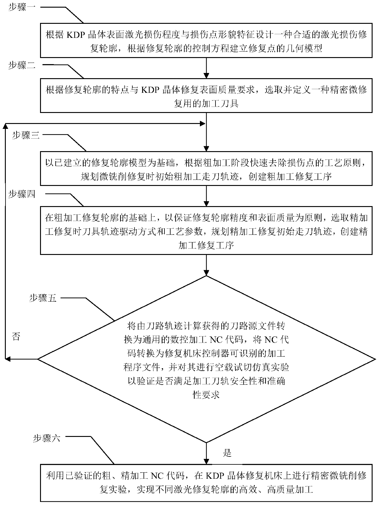
[0042] Specific implementation mode one: as Figure 1 to Figure 15 As shown, the implementation process of the micro-milling repair process method for laser damage on the surface of the large-diameter KDP crystal element described in this embodiment is:

[0043] Step 1. Design a suitable laser damage repair profile according to the laser damage degree on the KDP crystal surface and the shape characteristics of the damage point, and establish the geometric model of the repair point according to the control equation of the repair profile;

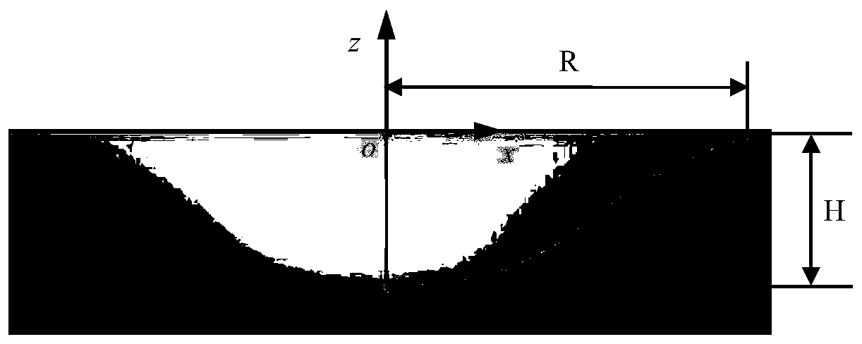
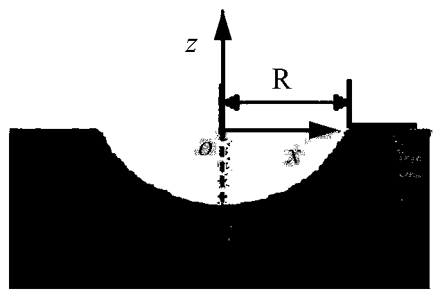
[0044] The laser damage repair profile described in step 1 mainly includes three forms: Gaussian, hemispherical and ellipsoidal. The repair profiles of these three forms are designed according to the morphology, size and distribution of laser damage points on the KDP crystal surface , for repairing the damaged surface with large damage area and small depth (ablation form), large damage point aspect ratio (pit, crack, etc.), and damage point l...


PUM

PropertyMeasurementUnit
surface roughnessaaaaaaaaaa
diameteraaaaaaaaaa
diameteraaaaaaaaaa

Abstract

The invention discloses a micro-milling repair technical method for the laser damage of the surface of a large-diameter KDP crystal element, and belongs to the technical field of repair machining of optical materials and optical elements in order to solve the problems that during repair of laser damage points of the surface of a soft and fragile KDP crystal element, the repair outline is simplex,the repaired surface quality is poor, and the efficiency is low. A geometric model of repairing points is built according to a control equation of the repair outline. A machining tool is selected. A rough machining repair procedure is built. A finish machining repair procedure is built. A tool path source file worked out according to the track of a tool path is converted into common numerical control machining NC codes, and the NC codes are converted into a machining program file capable of being recognized by a repair machine tool controller. A precise micro-milling repair experiment is carried out on a KDP crystal repair machine tool through the rough and finish machining NC codes, and efficient and high-quality machining of different laser friendly repairing outlines is realized. The increase behavior of laser damage points of the surface of the crystal element can be delayed, the laser damage resistance of the crystal element is improved, and the service life of the crystal elementis prolonged.

Description

technical field [0001] The invention belongs to the technical field of repairing and processing of optical materials and optical elements, and in particular relates to a precision micro-milling repairing process for laser damage points on the surface of large-diameter KDP crystal elements. Background technique [0002] KDP functional crystal materials should have unique optical properties and be used to make photoelectric switches and frequency doubling components, and become an irreplaceable core device in the current laser-driven inertial confinement fusion project. At present, the single-point diamond flying cutting ultra-precision machining technology can basically realize the processing and preparation of large-caliber, high-precision, high-quality crystal components. The processing accuracy and surface quality of engineering KDP crystal components have reached the limit level of mechanical processing. However, the processed crystal components are very easy to induce su...

Claims


Application Information

Patent Timeline
Patent Type & Authority Patents(China)
IPC IPC(8): G06F17/00B28D5/02B28D5/00
CPCB28D5/0064B28D5/02
Inventor 程健陈明君马文静杨浩刘启赵林杰王廷章刘志超王健许乔
Owner HARBIN INST OF TECH
Why Eureka
Try Eureka