A method and apparatus for controlling stress variation in a material layer formed via pulsed DC physcial vapor deposition

A technology to control pulse and stress changes, which is applied in the coating process of metal materials, microstructure devices composed of deformable elements, coatings, etc., and can solve problems such as uneven stress distribution

Pending Publication Date: 2018-11-02
SPTS TECH LTD
View PDF4 Cites 7 Cited by
  • Summary
  • Abstract
  • Description
  • Claims
  • Application Information

AI Technical Summary

Problems solved by technology

However, if figure 2 As shown, when the voltage difference increases, it can be found that the stress distribution becomes inhomogeneous due to the plasma distribution across the chamber

Method used


Image

  • A method and apparatus for controlling stress variation in a material layer formed via pulsed DC physcial vapor deposition
  • A method and apparatus for controlling stress variation in a material layer formed via pulsed DC physcial vapor deposition
  • A method and apparatus for controlling stress variation in a material layer formed via pulsed DC physcial vapor deposition

Examples


Embodiment Construction

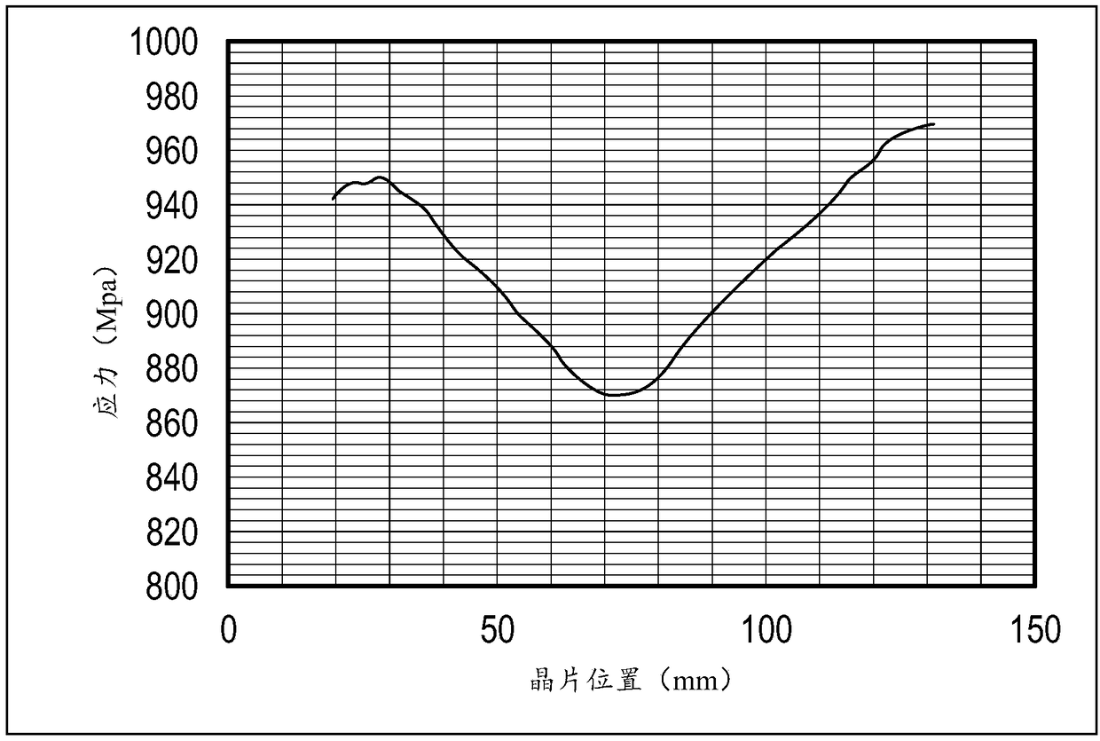
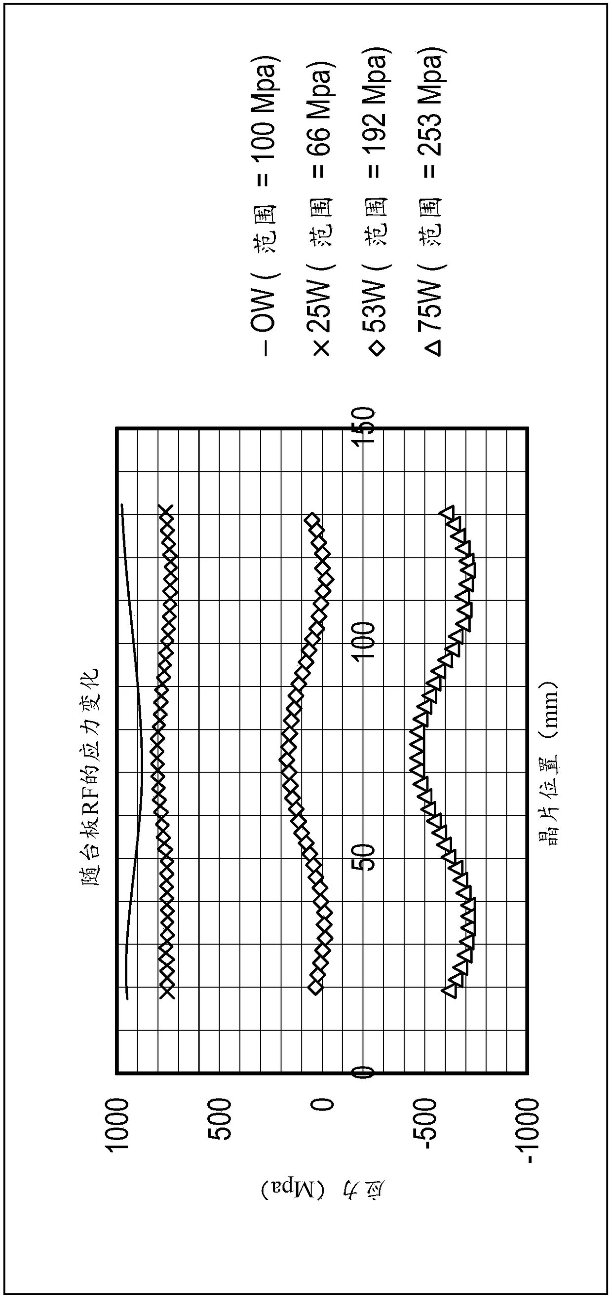
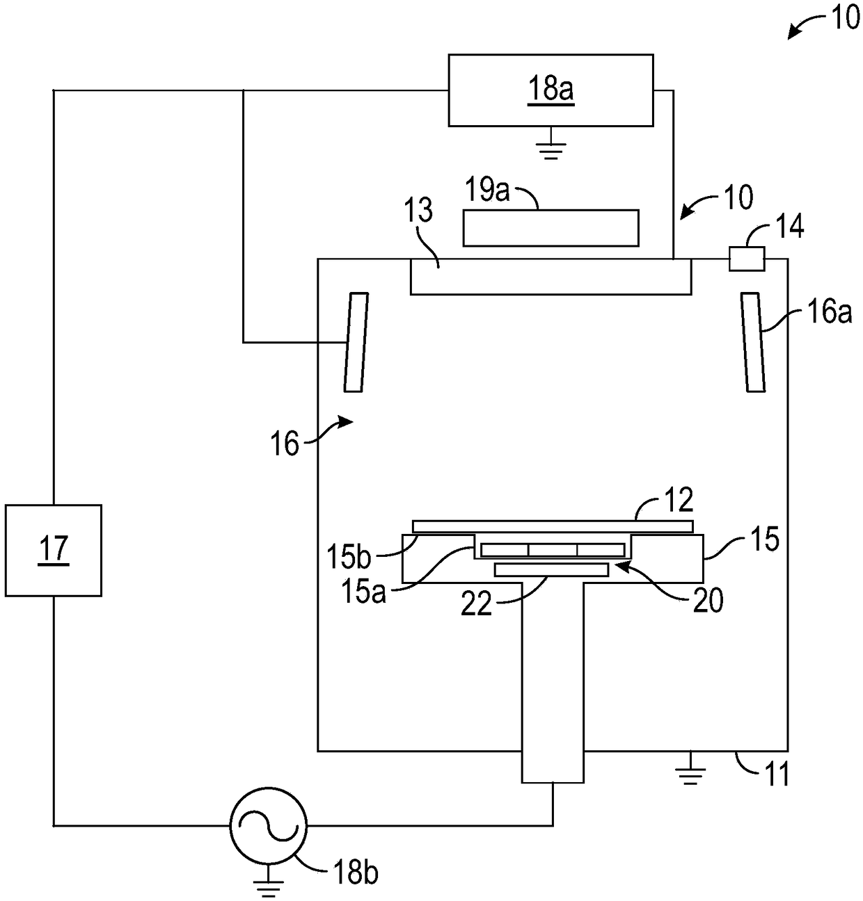
[0059] refer to image 3 , which shows a schematic diagram of an apparatus 10 for controlling stress variation in a material layer (not shown) formed on a substrate by physical vapor deposition according to an embodiment of the present invention. Apparatus 10 includes an electrically grounded processing chamber 11 within which a physical vapor deposition process takes place. The chamber 11 is arranged to house a substrate, such as a silicon wafer 12 , and source or target material 13 , which may include a metal planar layer, such as an aluminum disk, to form a sputtered layer on the wafer 12 . The chamber 11 also includes an inlet 14 for coupling to a gas source (not shown), such as, for example, the noble gases krypton, neon or argon, and a reactive gas such as nitrogen or oxygen to A nitride film or an oxide film is formed. Apparatus 10 also includes a platen 15 on which wafer 12 is located within chamber 11 . The platen 15 is placed within the chamber 11 so that the wafe...


PUM


Abstract

A method and apparatus is disclosed for controlling stress variation in a material layer formed via pulsed DC physical vapour deposition (PVD). The method comprises the steps of providing a chamber comprising a target from which the material layer is formed and a substrate upon which the material layer is formable, and subsequently introducing a gas within the chamber. The method further comprisesgenerating a plasma within the chamber and applying a first magnetic field proximate the target to substantially localise the plasma adjacent the target. An RF bias is applied to the substrate to attract gas ions from the plasma toward the substrate and a second magnetic field is applied proximate the substrate to steer gas ions from the plasma to selective regions upon the material layer formedon the substrate.

Description

technical field [0001] The invention relates to a method and equipment for controlling stress variation in a material layer formed by pulse direct current physical vapor deposition (PVD). Background technique [0002] Micro-Electro-Mechanical Systems (MEMS, Micro-Electro-Mechanical System) include devices that often exploit the piezoelectric properties of materials such as aluminum nitride and bimetallic nitrides (eg, aluminum nitride-scandium). This material is typically deposited on a substrate such as a wafer using physical vapor deposition techniques, and the distribution of stress within the material has been found to be a key factor affecting the operational characteristics of the device. Material deposition on a wafer can vary significantly, and as a result, devices formed on the same wafer often have different operating characteristics. [0003] In attempting to obtain uniform characteristics of devices formed on the wafer, the plasma distribution across the chamber...

Claims


Application Information

Patent Timeline
Patent Type & Authority Applications(China)
IPC IPC(8): C23C14/35
CPCC23C14/3485C23C14/351C23C14/352C23C14/50C23C14/505H01J37/32669H01J37/3452H01J37/32715H01J37/3467H01J37/347C23C14/3471H01L21/02178H01L21/02266B81B3/0072B81C2201/017B81C2201/0181C23C14/345H01J37/3408H01L21/02631H01L21/67017H01L21/67213H01J37/32174H05H1/46H01J37/3485H01L21/2855H01L21/76877
Inventor 安东尼·威尔比史蒂夫·伯吉斯I·蒙克里夫克莱夫·韦迪克斯斯科特·海莫尔R·辛德曼
Owner SPTS TECH LTD
Why Eureka
Try Eureka