Electronic device, manufacturing method of electronic device, and sputtering target

Inactive Publication Date: 2012-03-01
SEMICON ENERGY LAB CO LTD
View PDF2 Cites 29 Cited by
  • Summary
  • Abstract
  • Description
  • Claims
  • Application Information

AI Technical Summary

Benefits of technology

[0035]It is also found that the higher the temperature of the heat treatment is, the lower the pressure is, and the longer the heat treatment time is, the more easily zinc is vaporized from the oxide film and the concentration of zinc in the oxide film is decreased. When the

Problems solved by technology

However, when the conductivity of an oxide is decreased, it becomes difficult to employ a DC sputtering method or an AC sputtering method.
This is because when the conductivity of a target i

Method used


Image

  • Electronic device, manufacturing method of electronic device, and sputtering target
  • Electronic device, manufacturing method of electronic device, and sputtering target
  • Electronic device, manufacturing method of electronic device, and sputtering target

Examples


embodiment 1

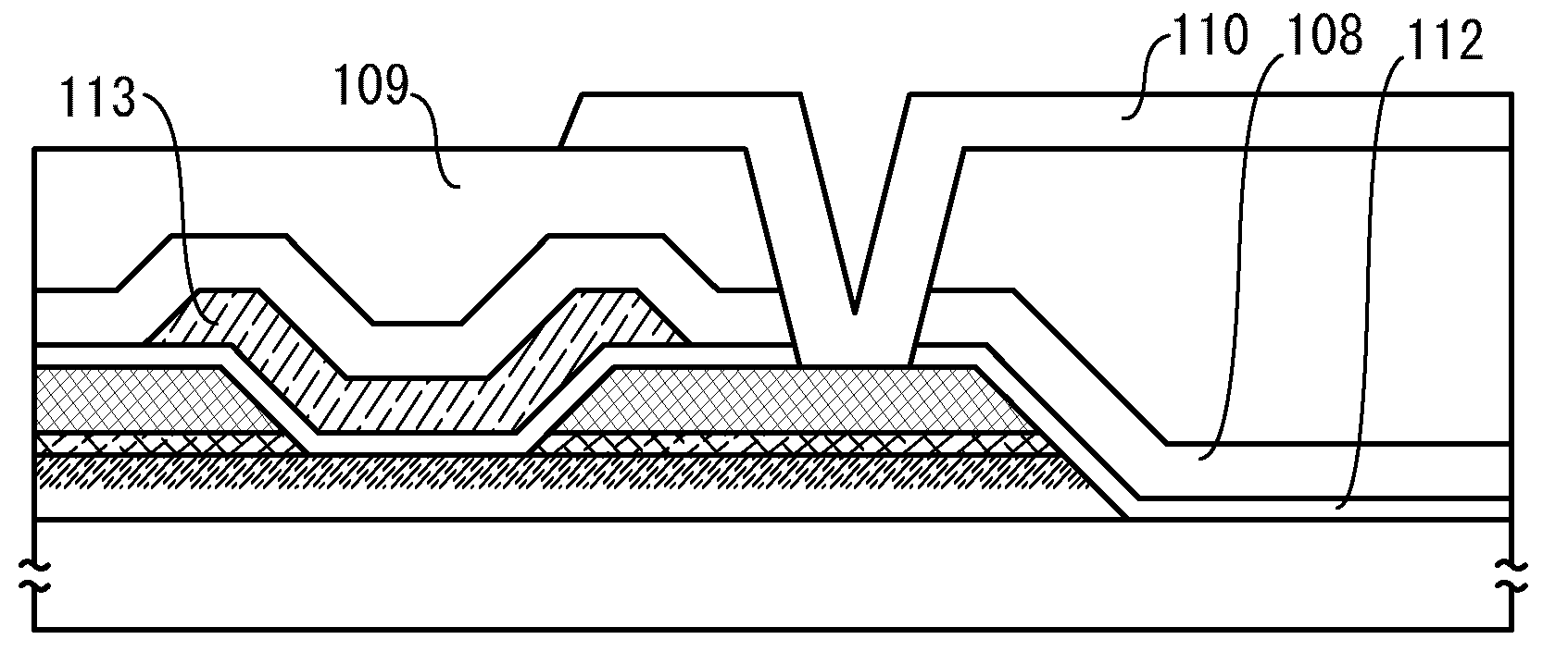
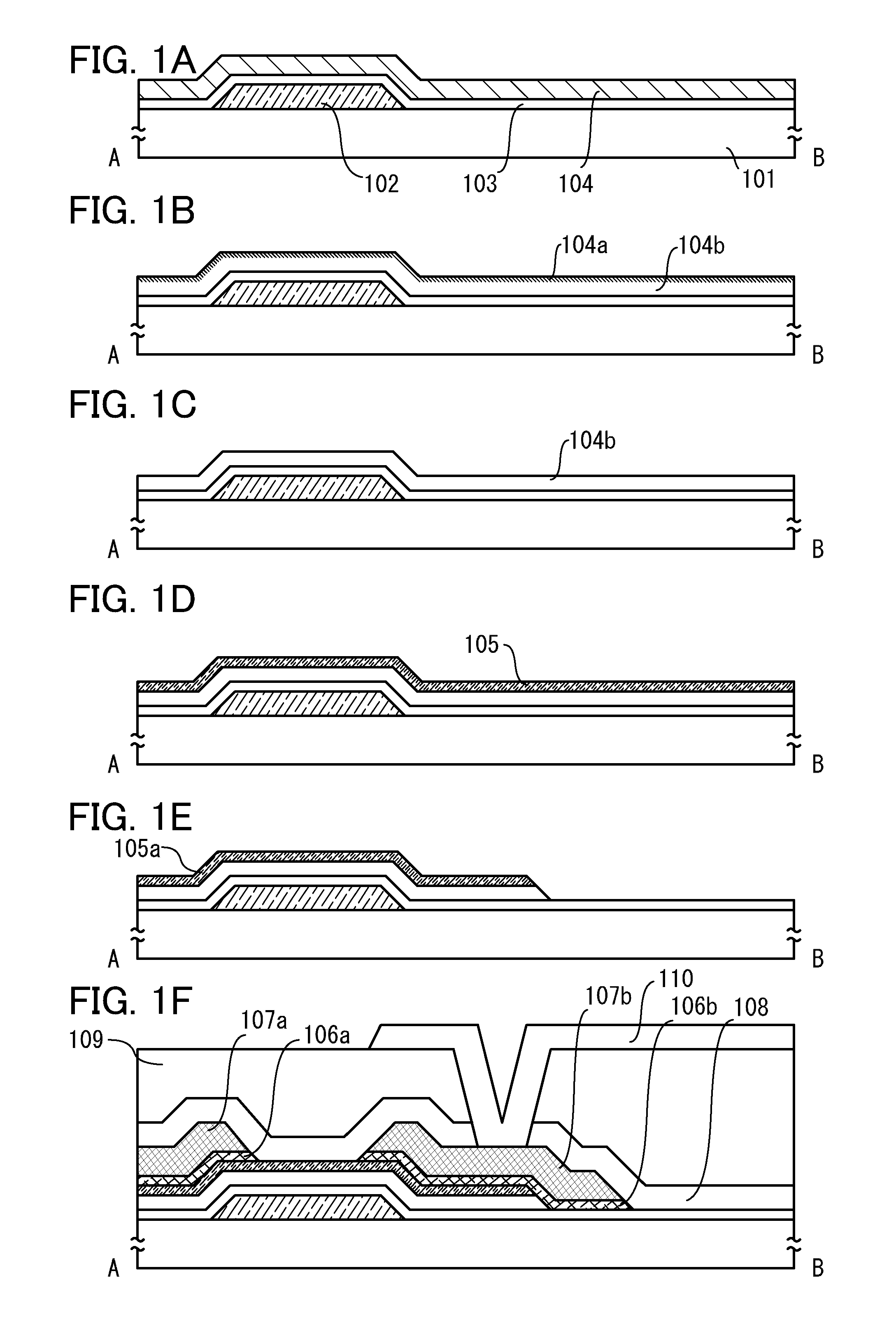
[0056]In this embodiment, an example in which a display device having a transistor is formed using the above-described technical idea will be described. FIGS. 1A to 1F are cross-sectional views illustrating a manufacturing process of the display device of this embodiment. The transistor described in this embodiment is a bottom-gate transistor whose gate electrode is located on the substrate side and a top-contact transistor whose source electrode and drain electrode are in contact with a top surface of a semiconductor layer, and a semi-conductive oxide is used as a semiconductor.

[0057]The outline of a manufacturing process will be described below. As illustrated in FIG. 1A, a gate electrode 102, a first gate insulator 103 of silicon oxide, silicon oxynitride, or the like, and an oxide film 104 are formed over a substrate 101 having an insulating surface. The first gate insulator 103 is not necessarily provided. In addition, the oxide film 104 is an oxide of gallium and zinc in this ...

embodiment 2

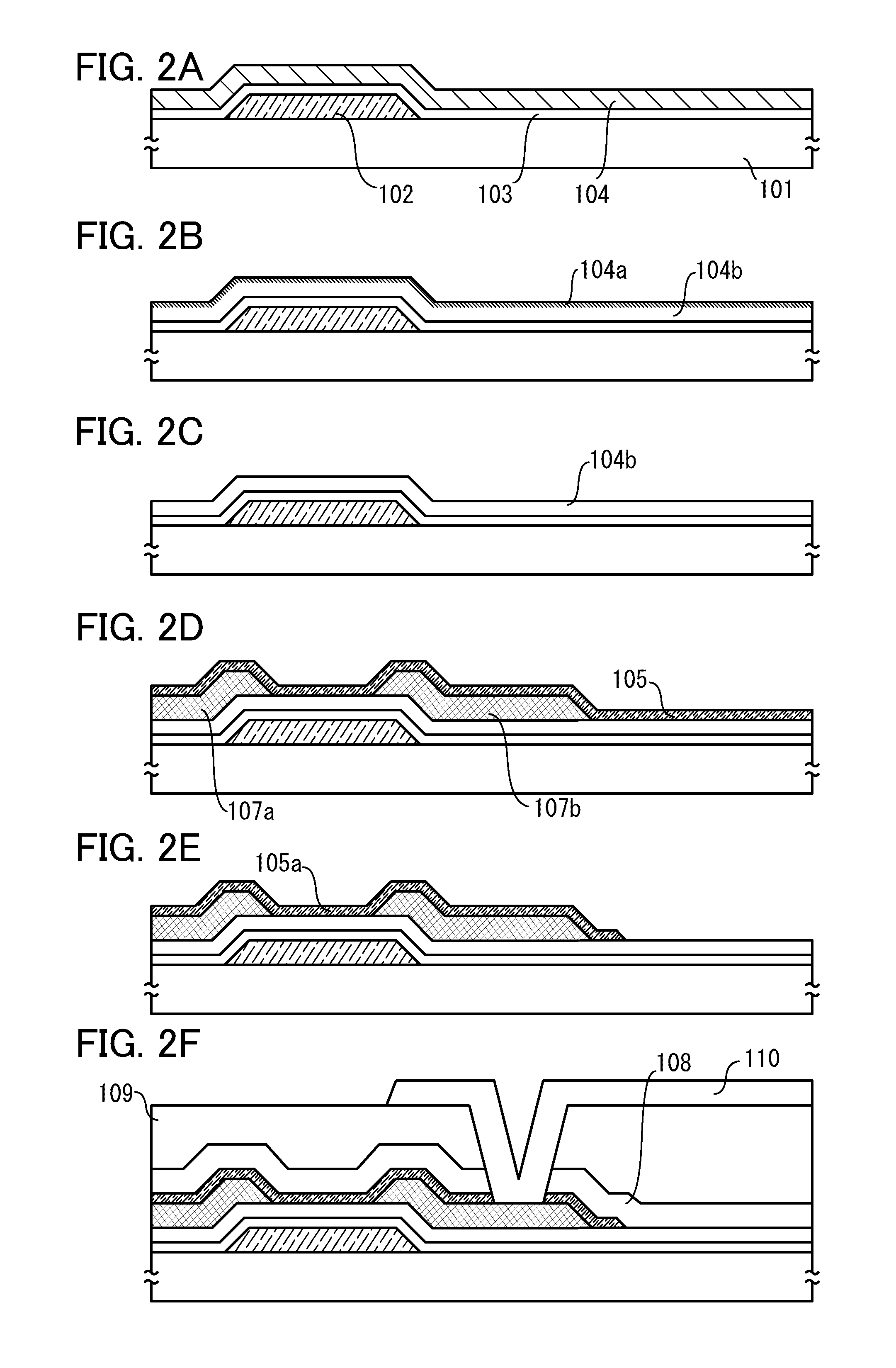
[0134]In this embodiment, an example in which a display device including a transistor having a different structure from the transistor described in Embodiment 1 is manufactured will be described. FIGS. 2A to 2F are cross-sectional views illustrating a manufacturing process of the display device of this embodiment. The transistor described in this embodiment includes a semi-conductive oxide as a semiconductor and is a bottom-gate transistor. In addition, the transistor described in this embodiment is a bottom-contact transistor whose source electrode and drain electrode are in contact with a lower surface of a semiconductor layer.

[0135]The outline of a manufacturing process will be described below. Note that for the structures denoted by the same reference numerals as those in Embodiment 1, a material, a means, a condition, and the like described in Embodiment 1 may be used as those in this embodiment unless otherwise specified. As illustrated in FIG. 2A, the gate electrode 102, the ...

embodiment 3

[0145]In this embodiment, an example in which a display device including a transistor having a different structure from the transistors described in the above embodiments is manufactured will be described. FIGS. 3A to 3F are cross-sectional views illustrating a manufacturing process of the display device of this embodiment. The transistor described in this embodiment includes a semi-conductive oxide as a semiconductor and is a top-gate transistor in which a gate is formed over a semiconductor layer. In addition, the transistor described in this embodiment is a top-contact transistor whose source electrode and drain electrode are in contact with an upper surface of a semiconductor layer.

[0146]The outline of a manufacturing process will be described below. Note that for the structures denoted by the same reference numerals as those in Embodiment 1, a material, a means, a condition, and the like described in Embodiment 1 may be used as those in this embodiment unless otherwise specifie...


PUM

PropertyMeasurementUnit
Temperatureaaaaaaaaaa
Fractionaaaaaaaaaa
Electrical conductivityaaaaaaaaaa

Abstract

A film formation is performed using a target in which a material which is volatilized more easily than gallium when heated at 400° C. to 700° C., such as zinc, is added to gallium oxide by a sputtering method with high mass-productivity which can be applied to a large-area substrate, such as a DC sputtering method or a pulsed DC sputtering method. This film is heated at 400° C. to 700° C., whereby the added material is segregated in the vicinity of a surface of the film. Another portion of the film has a decreased concentration of the added material and a sufficiently high insulating property; therefore, it can be used for a gate insulator of a semiconductor device, or the like.

Description

BACKGROUND OF THE INVENTION[0001]1. Field of the Invention[0002]The present invention relates to an electronic device including an oxide film, a manufacturing method of the electronic device, and a sputtering target used for manufacturing the oxide film.[0003]Note that an electronic device in this specification refers to any device that utilizes electric properties, and a semiconductor device that can function by utilizing semiconductor characteristics is included in the category of the electronic device. In addition, a device that utilizes electric properties (e.g., a capacitor, a coil, or a variety of electronic tubes), even when the device does not utilize semiconductor characteristics, is included in the category of the electronic device. Therefore, an electro-optical device, a semiconductor circuit, and an electronic appliance are all included in the electronic device.[0004]2. Description of the Related Art[0005]Oxides include oxides having a variety of properties, such as a co...

Claims


Application Information

Patent Timeline
IPC IPC(8): H01L29/22H01L21/36H05K13/00C23C14/34C23C14/08
CPCC23C14/08C23C14/3414H01L21/02554H01L21/02565H01L21/02631H01L29/4908H01L29/66742H01L29/66969H01L29/045H01L29/24H01L29/247H01L29/78693H01L29/7869H01L27/1225
Inventor YAMAZAKI, SHUNPEI
Owner SEMICON ENERGY LAB CO LTD
Why Eureka
Try Eureka