Praseodymium indium zinc oxide thin film transistor and preparation method thereof

A technology of oxide thin film and praseodymium indium zinc, which is applied in the direction of transistor, semiconductor/solid-state device manufacturing, semiconductor devices, etc., can solve the problems of difficult flexible devices, poorly flexible substrates, process transfer temperature resistance characteristics, etc., to achieve short time consumption, Effect of high current switching ratio and high mobility

Active Publication Date: 2018-11-02
SOUTH CHINA UNIV OF TECH
View PDF4 Cites 6 Cited by
  • Summary
  • Abstract
  • Description
  • Claims
  • Application Information

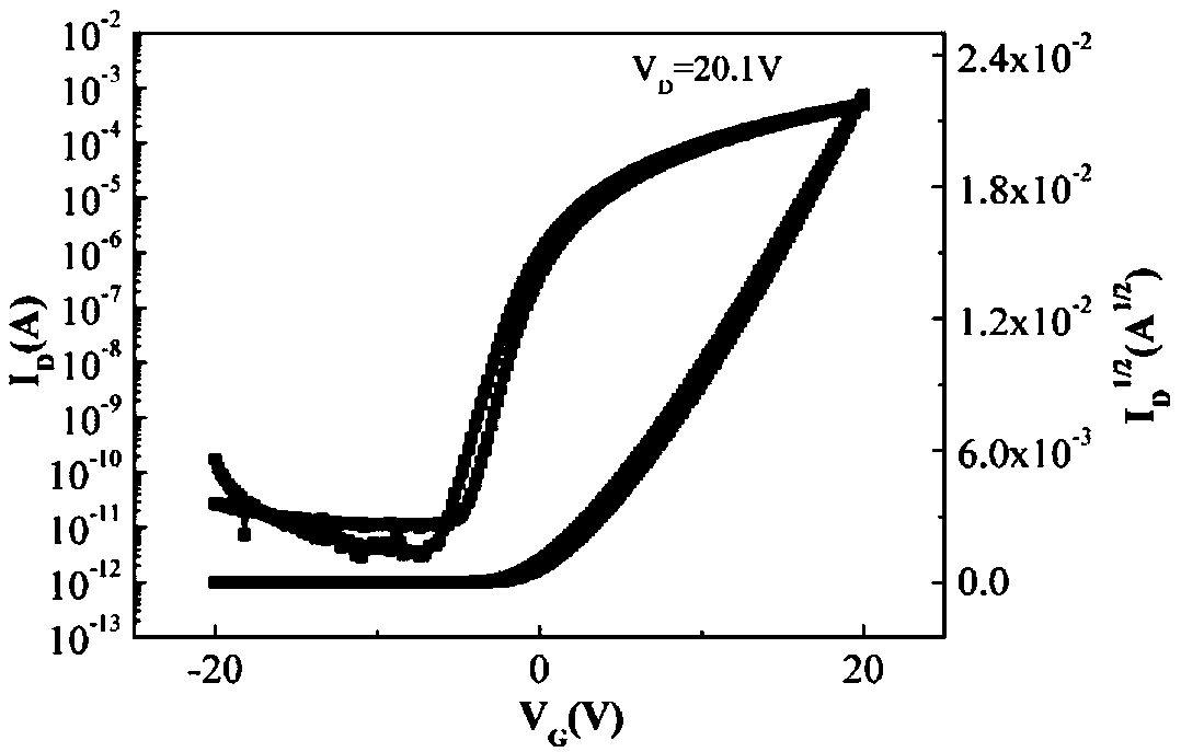
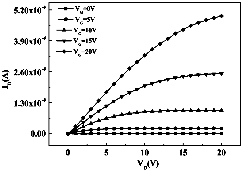
AI Technical Summary

Problems solved by technology

Usually, in order to improve the device performance of IGZO TFT, subsequent high-temperature treatment at around 300 °C is required, which is not conducive to transferring the process to flexible substrates with poor temperature resistance, and is difficult to further apply to the preparation of flexible devices.

Method used


Image

  • Praseodymium indium zinc oxide thin film transistor and preparation method thereof
  • Praseodymium indium zinc oxide thin film transistor and preparation method thereof
  • Praseodymium indium zinc oxide thin film transistor and preparation method thereof

Examples


Embodiment

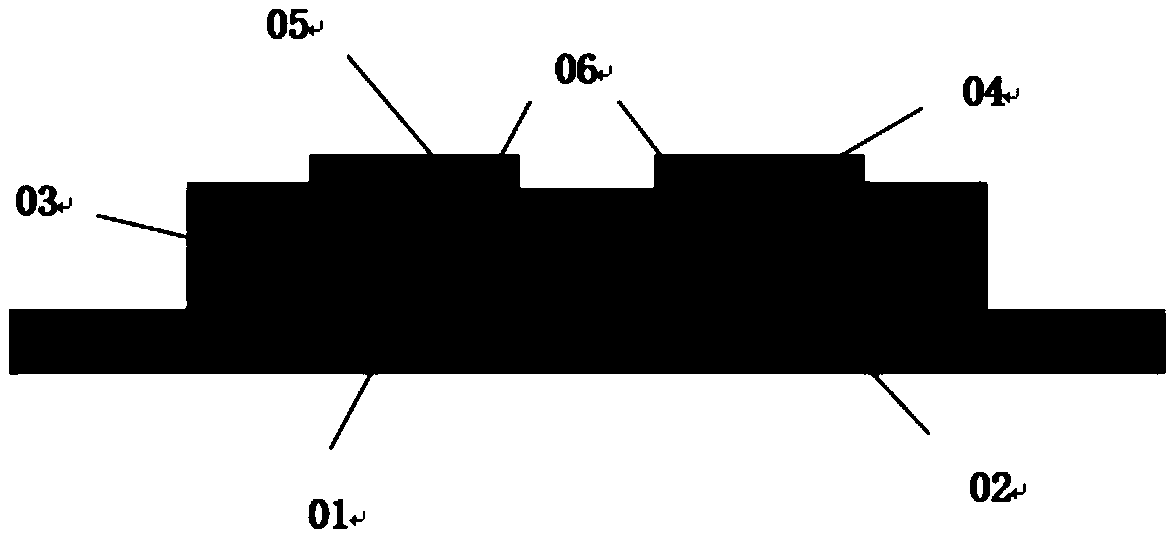
[0027] A praseodymium indium zinc oxide thin film transistor of this embodiment is prepared by the following method:

[0028] (1) Deposit a 300nm Al metal film on a glass substrate by DC sputtering at room temperature and pattern it with a mask as a gate;

[0029] (2) Oxidize 200nm Al in the gate to Al by anodic oxidation at room temperature 2 o 3 as a gate insulating layer;

[0030] (3) prepare the Pr-IZO semiconductor active layer by radio frequency sputtering at room temperature, the composition ratio of each material in the praseodymium indium zinc oxide (Pr 2 o 3 :In 2 o 3 : ZnO wt.%) is 3.9%: 86.4%: 9.7%. The total sputtering pressure is 3mtorr, and the sputtering atmosphere is Ar / O 2 =100 / 5 mixed gas, the radio frequency power supply is 80W, and the sputtering time is 129s; the thickness of the Pr-IZO semiconductor active layer obtained is about 6nm;

[0031] (4) Preparation of ultra-thin Al on the upper surface of the Pr-IZO semiconductor active layer by radio ...


PUM

PropertyMeasurementUnit
thicknessaaaaaaaaaa
thicknessaaaaaaaaaa
widthaaaaaaaaaa

Abstract

The invention belongs to the technical field of display devices, and discloses a praseodymium indium zinc oxide thin film transistor and a preparation method thereof. The thin film transistor is composed of a substrate, a metal gate, a gate insulating layer, a Pr-IZO semiconductor active layer, an oxide insulator passivation layer and metal source drain electrodes. Pr element doping is introducedinto the IZO semiconductor, and a Pr-IZO active layer thin film is deposited by a room temperature sputtering process; and by combination of an ultra-thin Al<2>O<3> passivation layer, carrier transportation under an electric field is controlled, so that the high-mobility and high-current-switching-ratio oxide thin film transistor can be realized at room temperature.

Description

technical field [0001] The invention belongs to the technical field of display devices, and in particular relates to a praseodymium indium zinc oxide thin film transistor and a preparation method thereof. Background technique [0002] Metal Oxide Thin Film Transistor (MOS TFT for short) has been widely studied in recent years because of its high mobility, good uniformity, good transparency to visible light and low temperature manufacturing process, and can be applied to display drivers such as LCD and AMOLED. middle. Oxide semiconductor is an important active layer material in TFT. It has high carrier concentration and strong charge transport ability, which can effectively drive TFT devices. At present, the widely used oxide active layer material is indium gallium zinc oxide (IGZO), and its device mobility is generally 10cm 2 / Vs. Usually, in order to improve the device performance of IGZO TFT, subsequent high-temperature treatment at around 300 °C is required, which is n...

Claims


Application Information

Patent Timeline
Patent Type & Authority Applications(China)
IPC IPC(8): H01L29/786H01L29/24H01L21/34
CPCH01L29/24H01L29/66969H01L29/7869
Inventor 宁洪龙张啸尘姚日晖卢宽宽刘贤哲邓宇熹李晓庆章红科徐苗彭俊彪
Owner SOUTH CHINA UNIV OF TECH
Why Eureka
Try Eureka