Multipurpose inductor-capacitor integrated structure

A multi-purpose, inductive technology, applied in the direction of electric solid-state devices, circuits, electrical components, etc., can solve the problem of occupying a large space, achieve the effect of reducing area and space, saving area and space, and remarkable functional characteristics

Active Publication Date: 2018-11-06
HARBIN INST OF TECH
View PDF4 Cites 3 Cited by
  • Summary
  • Abstract
  • Description
  • Claims
  • Application Information

AI Technical Summary

Problems solved by technology

However, DC choppers often need to use multiple inductors and capacitors in succession, which takes up a lot of space

Method used


Image

  • Multipurpose inductor-capacitor integrated structure
  • Multipurpose inductor-capacitor integrated structure
  • Multipurpose inductor-capacitor integrated structure

Examples


specific Embodiment approach 1

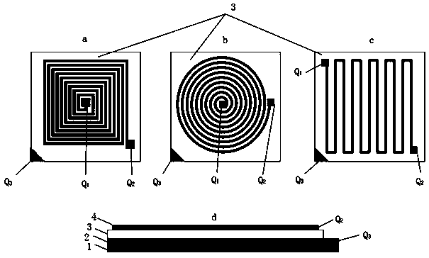
[0030] Specific implementation mode one: as figure 1 As shown, the multipurpose inductance-capacitance integrated structure provided by this embodiment is composed of a substrate 1, a conductive layer 2, a functional material film layer 3 and a conductive coil layer 4, wherein:

[0031] The substrate 1 is provided with a conductive layer 2;

[0032] The conductive layer 2 is used as the electrode Q of the lower layer of the capacitor 3 , which is provided with a functional material film layer 3;

[0033] The functional material thin film layer 3 is used as a capacitor dielectric layer and an inductive magnetic core, on which a conductive coil layer 4 is arranged;

[0034] The conductive coil layer 4 is used as an electrode on the upper layer of the capacitor, and the outer ring end of the conductive coil is used as the output signal terminal Q of the capacitor 2 , the inner end of the coil is used as the capacitor input signal end Q 1 .

[0035] Concrete preparation steps...

specific Embodiment approach 2

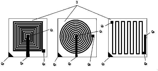
[0042] Embodiment 2: The difference between this embodiment and Embodiment 1 is that the functional material film layer 3 is composed of a dielectric material layer / magnetic material layer, and the dielectric material layer is arranged on the conductive layer 2. The conductive coil layer 4 is disposed on the dielectric material layer, and the magnetic material layer is disposed on the conductive coil layer 4 .

[0043] In this embodiment, the number of layers of the functional material thin film layer and the conductive coil layer is N layers (N is an integer greater than 1), and each layer of functional material thin film layer is provided between the dielectric material layer and the magnetic material layer. layer conductive coil layer. Concrete preparation steps are as follows:

[0044] 1. Prepare a conductive layer on the substrate;

[0045] 2. Prepare a dielectric material layer on the conductive layer;

[0046] 3. Prepare a conductive coil layer on the dielectric mate...

specific Embodiment approach 3

[0055] Specific embodiment three: the difference between this embodiment and specific embodiment two is that the dielectric material layer is disposed on the conductive layer 2, the magnetic material layer is disposed on the dielectric material layer, and the conductive coil layer 4 is disposed on the magnetic material layer superior.

[0056] In this embodiment, the number of layers of the functional material thin film layer and the conductive coil layer is N layers (N is an integer greater than 1), and each magnetic material layer is provided with a layer of conductive coil layer 4 . Concrete preparation steps are as follows:

[0057] 1. Prepare a conductive layer on the substrate;

[0058] 2. Prepare a dielectric material layer on the conductive layer;

[0059] 3. Preparing a magnetic material layer on the dielectric material layer;

[0060] 4. Prepare a conductive coil layer on the magnetic material layer;

[0061] 5. Prepare a dielectric material layer on the conducti...


PUM


Abstract

The invention discloses a multipurpose inductor-capacitor integrated structure comprising a substrate, a conductive layer, a thin film layer of a functional material and a conductive coil layer, and an upper surface of the substrate is provided with a conductive layer which is used as the lower layer electrode Q3 of the capacitor, the conductive lay is provided with a thin film layer of functionalmaterial on the upper surface thereof; the thin film layer of functional material is used as a capacitor dielectric layer and an inductive magnetic core, the thin film layer of the functional material is provided with a conductive coil layer on the upper surface; the conductive coil layer is used as the upper layer electrode of the capacitor, the outer coil end of the conductive coil is used as the capacitor output signal terminal Q2, and the inner coil end of the conductive coil is used as the capacitor input signal terminal Q1. The layer number which is at least one, of the thin film layersof the functional material is the same with that of the conductive coil layers. According to the invention, a plurality of electronic devices applied in integrated circuits can be formed by connecting other electronic components. The invention can greatly reduce the size of two passive devices of an inductor and a capacitor and has a significant impact on improvement of the microsystem integration.

Description

technical field [0001] The invention belongs to the field of integrated manufacturing of microelectronic systems, and relates to a multipurpose integrated structure of inductance and capacitance. Background technique [0002] In the past few decades, with the continuous advancement of information technology, electronic products have continued to develop in the direction of miniaturization and integration. System integration is an inevitable trend in the development of microelectronics. When integrated circuit chips follow Moore's law to develop toward higher integration and smaller line widths, off-chip discrete passive devices such as inductors and capacitors still occupy a large proportion of space in electronic systems. In order to further reduce the space occupied by the system and increase the degree of integration, it is necessary to realize the miniaturization and integration of off-chip discrete devices. As an important component of electronic circuits, the miniatur...

Claims


Application Information

Patent Timeline
Patent Type & Authority Applications(China)
IPC IPC(8): H01L23/64
CPCH01L23/642H01L23/645
Inventor 王春青梁新宇石宇皓石成杰
Owner HARBIN INST OF TECH
Why Eureka
Try Eureka